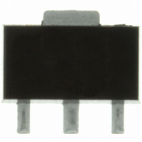
MMG3015NT1 Freescale Semiconductor, MMG3015NT1 Datasheet

MMG3015NT1
Specifications of MMG3015NT1
MMG3015NT1TR
Available stocks
Related parts for MMG3015NT1
MMG3015NT1 Summary of contents
Page 1
... CC C Document Number: MMG3015N Rev. 0, 8/2007 MMG3015NT1 0 - 6000 MHz, 15.5 dB 20.5 dBm InGaP HBT CASE 1514 - 02, STYLE 1 SOT - 89 PLASTIC Rating Symbol Value ( (2) I 300 +150 stg (3) T 150 J (4) Symbol Value R 41.5 θJC MMG3015NT1 Unit V mA dBm °C °C Unit °C/W 1 ...
Page 2
... Output Return Loss (S22) Power Output @ 1dB Compression Third Order Output Intercept Point Noise Figure (1) Supply Current (1) Supply Voltage 1. For reliable operation, the junction temperature should not exceed 150°C. MMG3015NT1 Vdc, 900 MHz 25°C, 50 ohm system, in Freescale Application Circuit Symbol G p ...
Page 3
... Charge Device Model (per JESD 22 - C101) Table 7. Moisture Sensitivity Level Test Methodology Per JESD 22 - A113, IPC/JEDEC J - STD - 020 RF Device Data Freescale Semiconductor Table 5. Functional Pin Description Pin Pin Function Number Ground 3 RF /DC Supply out Class 1C (Minimum) A (Minimum) IV (Minimum) Rating Package Peak Temperature 1 260 Unit °C MMG3015NT1 3 ...
Page 4
... Vdc OUTPUT POWER (dBm) out Figure 4. Small - Signal Gain versus Output Power 160 140 120 100 COLLECTOR VOLTAGE (V) CC Figure 6. Collector Current versus Collector Voltage MMG3015NT1 4 50 OHM TYPICAL CHARACTERISTICS 0 −5 −10 −15 −20 − Figure 3. Input/Output Loss versus Frequency 0 ...
Page 5
... Figure 13. Single - Carrier W - CDMA Adjacent Channel Power Ratio versus Output Power Vdc 900 MHz 1 MHz Tone Spacing − TEMPERATURE (_C) versus Case Temperature 125 130 135 140 145 T , JUNCTION TEMPERATURE (° Vdc Vdc mA 2140 MHz OUTPUT POWER (dBm) out MMG3015NT1 80 100 150 ...
Page 6
... Figure 15. S21, S11 and S22 versus Frequency Table 8. 50 Ohm Test Circuit Component Designations and Values Part C1, C2 0.01 μF Chip Capacitors C3 0.1 μF Chip Capacitor C4 1 μF Chip Capacitor L1 470 nH Chip Inductor 1/10 W Chip Resistor MMG3015NT1 6 V SUPPLY R1 L1 DUT 0.403″ ...
Page 7
... Getek Grade ML200C, 0.031″, ε Figure 17. 50 Ohm Test Circuit Schematic Vdc 2800 3200 3600 Figure 19. 50 Ohm Test Circuit Component Layout Description OUTPUT 4 MMG30XX Rev 2 Part Number Manufacturer C0603C151J5RAC Kemet C0603C104J5RAC Kemet C0603C105J5RAC Kemet HK160856NJ - T Taiyo Yuden CRCW06030000ZKEA Vishay MMG3015NT1 7 ...
Page 8
... MMG3015NT1 8 50 OHM TYPICAL CHARACTERISTICS = 5 Vdc mA 255C, 50 Ohm System ∠ φ 6.17 171.48 0.08 6.16 169.36 0.08 6 ...
Page 9
... T = 255C, 50 Ohm System) (continued ∠ φ 4.34 48.07 0.09 4.30 45.96 0.09 4.27 44.53 0.09 4.23 42.83 0.09 4.20 41.14 0. ∠ φ ∠ φ 47.31 0.49 139.46 - 48.32 0.50 137.08 - 49.01 0.50 135.57 - 49.82 0.51 133.81 - 50.64 0.52 132.08 MMG3015NT1 9 ...
Page 10
... Recommended Solder Stencil Figure 20. Recommended Mounting Configuration MMG3015NT1 10 7.62 1.27 NOTES: 1. THERMAL AND RF GROUNDING CONSIDERATIONS SHOULD BE USED IN PCB LAYOUT DESIGN. 2. DEPENDING ON PCB DESIGN RULES, AS MANY VIAS AS POSSIBLE SHOULD BE PLACED ON THE LANDING PATTERN VIAS CANNOT BE PLACED ON THE LANDING PATTERN, THEN ...
Page 11
... RF Device Data Freescale Semiconductor PACKAGE DIMENSIONS MMG3015NT1 11 ...
Page 12
... MMG3015NT1 12 RF Device Data Freescale Semiconductor ...
Page 13
... RF Device Data Freescale Semiconductor MMG3015NT1 13 ...
Page 14
... Application Notes • AN1955: Thermal Measurement Methodology of RF Power Amplifiers • AN3100: General Purpose Amplifier Biasing The following table summarizes revisions to this document. Revision Date 0 Aug. 2007 • Initial Release of Data Sheet MMG3015NT1 14 PRODUCT DOCUMENTATION REVISION HISTORY Description RF Device Data Freescale Semiconductor ...
Page 15
... Freescale Semiconductor was negligent regarding the design or manufacture of the part. Freescalet and the Freescale logo are trademarks of Freescale Semiconductor, Inc. All other product or service names are the property of their respective owners. © Freescale Semiconductor, Inc. 2007. All rights reserved. MMG3015NT1 15 ...


