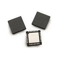
MGA-43328-BLKG Avago Technologies US Inc., MGA-43328-BLKG Datasheet - Page 15

MGA-43328-BLKG
Manufacturer Part Number
MGA-43328-BLKG
Description
IC PWR AMP 2.5-2.7GHZ 28QFN
Manufacturer
Avago Technologies US Inc.
Type
High Linearity Amplifierr
Datasheet
1.MGA-43328-TR1G.pdf
(19 pages)
Specifications of MGA-43328-BLKG
P1db
35.5dBm
Noise Figure
2.1dB
Package / Case
28-VFQFN Exposed Pad
Current - Supply
470mA
Frequency
2.5GHz ~ 2.7GHz
Gain
37.3dB
Rf Type
802.16 WiMAX
Test Frequency
2.6GHz
Voltage - Supply
5V
Bandwidth
2.5 GHz to 2.7 GHz
Mounting Style
SMD/SMT
Number Of Channels
1
Operating Supply Voltage
5 V
Supply Current
470 mA
Maximum Power Dissipation
8 W
Lead Free Status / RoHS Status
Lead free / RoHS Compliant
Lead Free Status / RoHS Status
Lead free / RoHS Compliant, Lead free / RoHS Compliant
Application Schematic
Figure 36. Application schematic in demonstration board
Notes:
1. In normal gain mode operation, Vbyp = 0V. Vc1, Vc2 and Vc3 are bias pins that are used to set the bias conditions to the 3 internal gain stages of
2. Typical quiescent current distribution with Vdd1 = Vdd2 = Vdd3 = Vbias = 5V, Vbyp = 0V, Vc = 2.1V is :
3. Low gain mode is enabled by setting Vbyp pin to 5V. This condition overrides the normal high gain mode operation and bypasses the first gain
4. Modulated signal measurements are made with Agilent 89600 VSA and Agilent E4438C signal generator with IEEE 802.16e option using the
5. Typical operating voltages and currents:
6. Vdd1/2/3 are shown as separate supplies with individual bypass capacitors. This yields the most stable configuration. If a common power supply
15
the PA.
a. Idd1 = 55.5 mA
b. Idd2 = 146 mA
c. Idd3 = 268.5 mA
d. Ibias = 16.5mA
(Note: Vc supplied through Vc2 pin on demonstration board with R2 = 1.0k: , R3 = 390: and R4 = 1.1k:)
stage, regardless of the voltage at Vc1 pin.
following test conditions :
– Signal format: IEEE 802.16e OFDMA, ¾ rate FEC
– Modulation: 64-QAM
– Number of Subcarriers: 840
– Modulation bandwidth: 10 MHz
– Downlink ratio: 50%
Residual distortion of signal generator: (0.6-0.8)%. This distortion is not removed from the overall EVM data in the datasheet.
a. Normal gain mode : Vdd1 = Vdd2 = Vdd3 = Vbias = 5V. Vc = 2.1V. Vbyp = 0V. Iq(total) = 470 mA.
b. Low gain mode : Vdd1 = Vdd2 = Vdd3 = Vbias = 5V. Vc = 2.1V. Vbyp = 5V. Iq(total) = 470 mA.
line is used, proper broadband bypass decoupling is recommended to reduce common mode feedback through the supply line.


