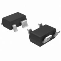
MGA-53543-TR2G Avago Technologies US Inc., MGA-53543-TR2G Datasheet - Page 11

MGA-53543-TR2G
Manufacturer Part Number
MGA-53543-TR2G
Description
IC AMP RFIC GAAS 1.9GHZ SOT-343
Manufacturer
Avago Technologies US Inc.
Type
General Purpose Amplifierr
Datasheet
1.MGA-53543-TR1G.pdf
(14 pages)
Specifications of MGA-53543-TR2G
P1db
18.6dBm
Noise Figure
1.5dB ~ 1.9dB
Package / Case
SC-70-4, SC-82-4, SOT-323-4, SOT-343
Current - Supply
40mA ~ 70mA
Frequency
50MHz ~ 6GHz
Gain
14dB ~ 17dB
Rf Type
Cellular, PCS, WLL, WLAN
Test Frequency
1.9GHz
Voltage - Supply
5V
Operating Frequency
50 MHz to 6 GHz
Operating Supply Voltage
5.5 V
Supply Current
70 mA
Maximum Power Dissipation
400 mW
Maximum Operating Temperature
+ 150 C
Mounting Style
SMD/SMT
Number Of Channels
1 Channel
Manufacturer's Type
Linear Amplifier
Frequency (max)
6GHz
Operating Supply Voltage (max)
5.5V
Package Type
SOT-343
Mounting
Surface Mount
Pin Count
3 +Tab
Noise Figure (typ)
1.9@2400MHzdB
Lead Free Status / RoHS Status
Lead free / RoHS Compliant
Lead Free Status / RoHS Status
Lead free / RoHS Compliant, Lead free / RoHS Compliant
Available stocks
Company
Part Number
Manufacturer
Quantity
Price
Part Number:
MGA-53543-TR2G
Manufacturer:
AVAGO/安华高
Quantity:
20 000
900 MHz LNA Design
To demonstrate the versatility of the MGA-53543, the
following example describes a cellular band Low Noise
Amplifier (LNA) design. The methodology for a 900 MHz
LNA design differs from the previous examples in that
only the input match affects noise figure. Thus, optimiz-
ing for minimum noise figure entails matching only the
input to Γ
matched to S for better gain or Γ
Figure 7 shows the complete schematic for a 900 MHz
low noise amplifier design and Table 5 describes the re-
quired components.
RF
Figure 27. Schematic for 900 MHz LNA design.
Table 5. Component Parts List for the MGA-53543 HLA at 900 MHz.
1 nH
15 nH
4.7 pF
.Ω
1000 pF Phycomp 040R10K9B00
Performance of MGA-53543 at 900 MHz
Biased with a +5 Volt supply MGA-53543 delivers a Noise
Figure of 1.33 dB at 900 MHz. This number is higher than
NF
ponents with parasitic losses. A microstip or distributed
element match may improve noise figure by . dB. Gain is
measured to be 17.4 dB as shown in Figure 8. Input and
output VSWR are both better than :1, with input return
loss of 5 dB and output return loss at 17.5 dB shown in
Figure 9.
11
in
min
only because of loss from lumped element com-
12 nH
TOKO LL1608-FS1NJ
TOKO LL1005-FS15N
Phycomp 040CG479C9B00
RHOM MCR01JR
4.7 pF
opt
instead of Γ
1
3
53
2
4
+5V
S
, and the output can either be
2.2Ω
15 nH
4.7 pF
1000 pF
RF
out
L
for better linearity.
Figure 28. Gain, Noise Figure and Output Power at 900 MHz.
Figure 29. Input and Output return loss at 900 MHz.
Input IIP3 is measured to be 18.6 dBm and P1dB is 19.0
dB at 900 MHz.
Figure 19. Gain, Noise Figure and Output
Power at 900 MHz.
Figure 20. Input and Output Return Loss at
900 MHz.
-10
-15
-20
-25
-30
20
15
10
-5
5
0
0
400
400
600
600
FREQUENCY (MHz)
FREQUENCY (MHz)
800
800
1000
1000
Gain
NF
1200
1200
S11
S22
1400
1400


