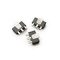
MGA-30889-BLKG Avago Technologies US Inc., MGA-30889-BLKG Datasheet - Page 2

MGA-30889-BLKG
Manufacturer Part Number
MGA-30889-BLKG
Description
IC AMP MMIC 40MHZ-2600MHZ SOT89
Manufacturer
Avago Technologies US Inc.
Type
Gain Block Amplifierr
Datasheet
1.MGA-30889-TR1G.pdf
(14 pages)
Specifications of MGA-30889-BLKG
P1db
20.3dBm
Noise Figure
2dB
Package / Case
TO-243-3, SC-62, SOT-89
Current - Supply
65mA
Frequency
40MHz ~ 2.6GHz
Gain
15.7dB
Rf Type
General Purpose
Test Frequency
1.95GHz
Voltage - Supply
5V
Mounting Style
SMD/SMT
Operating Frequency
40 MHz to 2600 MHz
Operating Supply Voltage
5 V
Supply Current
65mA
Maximum Power Dissipation
0.47 W
Manufacturer's Type
MMIC Amplifier
Number Of Channels
1
Frequency (max)
2.6GHz
Operating Supply Voltage (typ)
5V
Operating Supply Voltage (max)
5.5V
Package Type
SOT-89
Mounting
Surface Mount
Pin Count
3 +Tab
Noise Figure (typ)
2@1950MHzdB
Lead Free Status / RoHS Status
Lead free / RoHS Compliant
Lead Free Status / RoHS Status
Lead free / RoHS Compliant, Lead free / RoHS Compliant
Available stocks
Company
Part Number
Manufacturer
Quantity
Price
Company:
Part Number:
MGA-30889-BLKG
Manufacturer:
AVAGO
Quantity:
298
Absolute Maximum Rating
Product Consistency Distribution Charts
Figure 1. Ids, LSL=53mA , nominal=65mA, USL=77mA
Figure 3. OIP3, LSL=33dBm, nominal=36dBm
Figure 5. NF, nominal=2dB, USL=2.7dB
2
1.6
Symbol
V
P
P
T
T
diss
j,MAX
STG
dd,max
in,max
33
LSL
LSL
1.7
1.8
34
Parameter
Device Voltage, RF output to ground
CW RF Input Power
Total Power Dissipation
Junction Temperature
Storage Temperature
1.9
60
2
35
2.1 2.2
[1]
T
36
A
=25°C
2.3 2.4 2.5 2.6 2.7
[3]
37
70
[1, 2]
38
USL
USL
Units
V
dBm
W
°C
°C
39
Absolute Max.
5.5
20
0.47
150
-65 to 150
14.5
Figure 2. Gain, LSL=14.6dB, nominal=15.7dB, USL=16.8dB
Figure 4. P1dB, LSL=19.2dBm, nominal=20.3dBm
Notes:
1. Distribution data sample size is 3000 samples taken from 3 diff erent
2. Measurements were made on a characterization test board, which
19.2
wafer lots. Future wafers allocated to this product may have nominal
values anywhere between the upper and lower limits.
represents a trade-off between optimal OIP3, gain and P1dB. Circuit
trace losses have not been de-embedded from measurements
above.
LSL
LSL
15
19.6
Thermal Resistance
Notes:
1. Operation of this device in excess of any of
2. Thermal resistance measured using Infrared
3. This is limited by maximum Vdd and Ids.
Thermal Resistance
(Vdd = 5 V, Ids = 57.5 mA, Tc = 85°C)
15.5
these limits may cause permanent damage.
measurement technique.
Derate 13.2 mW/°C for Tc >114°C.
20
16
20.4
[2]
T
JC
= 76°C/W
16.5
20.8
USL


