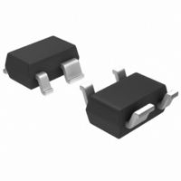
MGA-52543-TR2G Avago Technologies US Inc., MGA-52543-TR2G Datasheet - Page 2

MGA-52543-TR2G
Manufacturer Part Number
MGA-52543-TR2G
Description
IC AMP MMIC LNA 1.5GHZ SOT-343
Manufacturer
Avago Technologies US Inc.
Type
General Purpose Amplifierr
Datasheet
1.MGA-52543-TR2G.pdf
(8 pages)
Specifications of MGA-52543-TR2G
P1db
17.4dBm
Noise Figure
1.9dB ~ 2.3dB
Package / Case
SC-70-4, SC-82-4, SOT-323-4, SOT-343
Current - Supply
45mA ~ 65mA
Frequency
400MHz ~ 6GHz
Gain
13dB ~ 15.5dB
Rf Type
Cellular, PCS, WLL, WLAN
Test Frequency
1.9GHz
Voltage - Supply
4.5V ~ 5.5V
Operating Frequency
0.4 GHz to 10 GHz
Operating Supply Voltage
7 V
Supply Current
65 mA
Maximum Power Dissipation
425 mW
Maximum Operating Temperature
+ 160 C
Mounting Style
SMD/SMT
Number Of Channels
1 Channel
Lead Free Status / RoHS Status
Lead free / RoHS Compliant
Available stocks
Company
Part Number
Manufacturer
Quantity
Price
Part Number:
MGA-52543-TR2G
Manufacturer:
AVAGO/安华高
Quantity:
20 000
MGA-52543 Absolute Maximum Ratings
Electrical Specifications
T
Notes:
1. Measurements obtained from a fixed narrow band tuning described in Figure 1. This circuit designed to optimize Noise Figure and IIP3 while
2. Minimum Noise Figure and Associated Gain at F
3. Standard deviation data are based on at least 400 part sample size and 11 wafer lots.
Figure 1. Block Diagram of Test Fixture.
See Figure 7 in the Applications section for an equivalent schematic of 1.9 GHz circuit; Figure 11 in the Applications section for 900 MHz circuit.
2
Symbol
V
V
P
P
T
T
Symbol
I
NF
Gain
IIP3
F
G
OIP3
P
RL
RL
ISOL
RF
Input
c
d
STG
min
d
d
d
in
j
1dB
= +25°C, Z
a
test
maintaining VSWR better than 2:1.
system.
[2]
out
in
[1]
[2]
[1]
[1]
[1]
[1]
[1]
[1]
[1]
o
Parameter
Maximum Input Voltage
Supply Voltage
Power Dissipation
CW RF Input Power
Junction Temperature
Storage Temperature
= 50 Ω, V
Input
Match
Parameter and Test Condition
Current drawn
Noise Figure
Gain
Input Third Order Intercept Point
Minimum Noise Figure
Associated Gain at F
Output Third Order Intercept Point
Output Power at 1 dB Gain Compression 1.9 GHz
Input Return Loss
Output Return Loss
Isolation |s
d
= 5V, unless noted
12
|
2
[2,3]
min
[1]
Units
V
V
mW
dBm
°C
°C
min
computed from S-parameter and Noise Parameter data measured in an automated NF
Output Match
and DC Bias
Frequency
N/A
1.9 GHz
0.9 GHz
1.9 GHz
0.9 GHz
1.9 GHz
0.9 GHz
1.9 GHz
0.9 GHz
1.9 GHz
0.9 GHz
1.9 GHz
0.9 GHz
0.9 GHz
1.9 GHz
0.9 GHz
1.9 GHz
0.9 GHz
1.9 GHz
0.9 GHz
Absolute Maximum
±0.5
7.0
425
+20
160
-65 to 150
RF
Output
V
d
Units
mA
dB
dB
dBm
dB
dB
dBm
dBm
dB
dB
dB
Thermal Resistance:
T
Notes:
1. Operation of this device in excess of any
2. T
jc
Min.
45
13
14
= 150°C/W
of these limits may cause permanent
damage.
case
= 25°C
53
1.9
1.8
14.2
15
+17.5
+18
1.6
1.5
15.0
16.2
31.7
33.0
+17.4
+18
11
15
20
22
-25
-25
Typ.
[2]
2.3
15.5
Max.
70
V
3.57
0.15
0.26
2.28
[3]


