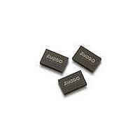
MGA-685T6-TR1G Avago Technologies US Inc., MGA-685T6-TR1G Datasheet - Page 2

MGA-685T6-TR1G
Manufacturer Part Number
MGA-685T6-TR1G
Description
IC RF AMP LNA GAAS MMIC 6-UTSLP
Manufacturer
Avago Technologies US Inc.
Type
General Purpose Amplifierr
Datasheet
1.MGA-685T6-TR2G.pdf
(20 pages)
Specifications of MGA-685T6-TR1G
Noise Figure
0.9dB
Package / Case
6-XFDFN Exposed Pad
Current - Supply
10mA
Frequency
100MHz ~ 1.5GHz
Gain
19dB
P1db
17.3dBm
Test Frequency
500MHz
Voltage - Supply
3.3V
Mounting Style
SMD/SMT
Number Of Channels
1
Operating Frequency
1500 MHz
Operating Supply Voltage
3 V
Supply Current
16 mA @ 3 V
Maximum Power Dissipation
600 mW
Manufacturer's Type
Low Noise Amplifier
Frequency (max)
1.5GHz
Operating Supply Voltage (typ)
3V
Package Type
UTSLP
Mounting
Surface Mount
Pin Count
6
Noise Figure (typ)
0.93@500MHzdB
Lead Free Status / RoHS Status
Lead free / RoHS Compliant
Rf Type
-
Lead Free Status / Rohs Status
Lead free / RoHS Compliant
Available stocks
Company
Part Number
Manufacturer
Quantity
Price
Company:
Part Number:
MGA-685T6-TR1G
Manufacturer:
NXP
Quantity:
12 000
Company:
Part Number:
MGA-685T6-TR1G
Manufacturer:
AVAGO
Quantity:
2 782
Part Number:
MGA-685T6-TR1G
Manufacturer:
AVAGO/安华高
Quantity:
20 000
Table 1. Absolute Maximum Rating
Notes:
1. Operation of this device above any one of there parameters may cause permanent damage.
2. Bias is assumed DC quiescent conditions.
3. With the DC (typical bias) and RF applied to the device at board temperature T
4. Total dissipation power is referred to board temperature, T
5. Thermal resistance is measured from junction to board using IR method.
Table 2. Electrical Specifi cations
T
Notes:
1. Circuit losses have been de-embedded from actual measurements.
2. Measurement in table 2 uses the test board and circuit schematic shows in fi gure 1a. Data based on 500 part sample size from two wafer lots
3. 0.5 GHz OIP3 Test Condition : F1 = 0.5 GHz, F2 = 0.505 GHz, Pin = -20 dBm
2
Symbol
Vd
Id
P
I
P
T
T
θ
Symbol
Id
NF
Gain
OIP3
P1dB
IRL
ORL
A
ref
diss
CH
STG
in,max
ch_b
= 25 °C, Freq = 0.5 GHz, Vd = 3V (unless otherwise specifi ed)
during initial characterization of this product.
[1,2]
[1,2]
[1,2]
[1,2]
[1,2]
[1,2,3]
[1,2]
Parameter
Device Current
Noise Figure in test circuit
Associated Gain in test circuit
Output 3rd Order Intercept in test circuit
Output Power at 1dB Gain Compression in test
circuit
Input Return Loss in test circuit
Output Return Loss in test circuit
Parameter
Device Voltage (Pin 5)
Device Current (Pin 5)
CW RF Input Power (Pin 2)
Bias Reference Current (Pin 6)
Total Power Dissipation
Channel Temperature
Storage Temperature
Thermal Resistance
[5]
[2]
[2]
[1]
[4]
[3]
B
= 92 °C, derate P
Units
mA
dB
dB
dBm
dBm
dB
dB
Units
V
mA
dBm
mA
mW
°C
°C
°C / W
diss
B
= 25 °C.
at 10 mW/ °C for T
Absolute Max.
6
100
+21
12
600
150
150
97
Min.
7
-
17.50
16.50
-
-
-
B
> 92 °C.
Typ
10
0.93
18.90
18.70
17.30
-8.10
-16.40
Max.
16
1.50
20.50
-
-
-
-


