ADA-4789-BLKG Avago Technologies US Inc., ADA-4789-BLKG Datasheet

IC AMP DARL BIPO 2.5GHZ SOT-89

ADA-4789-BLKG

Manufacturer Part Number
ADA-4789-BLKG
Description
IC AMP DARL BIPO 2.5GHZ SOT-89
Manufacturer
Avago Technologies US Inc.
Datasheet

Specifications of ADA-4789-BLKG

Gain
16.2dB
Rf Type
WLL, WLAN
Current - Supply
90mA
Frequency
0Hz ~ 2.5GHz
Noise Figure
4.4dB
P1db
16.2dBm
Package / Case
SC-62, SOT-89, TO-243 (3 Leads + Tab)
Test Frequency
2GHz
Voltage - Supply
3.3V ~ 4.3V
Frequency Range
DC To 2.5GHz
Noise Figure Typ
4.2dB
Power Dissipation Pd
370mW
Supply Current
60mA
Supply Voltage Range
3.3V To 4.3V
Number Of Channels
1
Frequency (max)
2.5GHz
Operating Supply Voltage (min)
3.3V
Operating Supply Voltage (typ)
3.8V
Operating Supply Voltage (max)
4.3V
Package Type
SOT-89
Mounting
Surface Mount
Pin Count
3 +Tab
Noise Figure (typ)
4.5@2000MHzdB
Lead Free Status / RoHS Status
Lead free / RoHS Compliant
Lead Free Status / RoHS Status
Lead free / RoHS Compliant, Lead free / RoHS Compliant

Available stocks

Company
Part Number
Manufacturer
Quantity
Price
Part Number:
ADA-4789-BLKG
Manufacturer:
AVAGO/安华高
Quantity:
20 000
ADA-4789
Silicon Bipolar Darlington Amplifier
Data Sheet
Description
Avago Technologies’ ADA-4789 is an economical, easy-
to-use, general purpose silicon bipolar RFIC gain block
amplifiers housed in SOT-89 surface mount plastic
package.
The Darlington feedback structure provides inherent
broad bandwidth performance, resulting in useful
operating frequency up to 2.5 GHz. This is an ideal
device for small-signal gain cascades or IF amplification.
ADA-4789 is fabricated using Avago’s HP25 silicon
bipolar process, which employs a double-diffused
single poly-silicon process with self-aligned submicron
emitter geometry. The process is capable of
simultaneous high fT and high NPN breakdown (25 GHz
fT at 6V BVCEO). The process utilizes industry standard
device oxide isolation technologies and submicron
aluminum multi-layer inter-connects to achieve
superior performance, high uniformity, and proven
reliability.
Package Marking and Pin Connections
Note: Package marking provides orientation and identification
“4G” = Device Code
“x” = Month code indicates the month of manufacture
• • • • • Small Signal Gain Amplifier
• • • • • Operating Frequency: DC – 2.5 GHz
• • • • • Unconditionally Stable
• • • • • 50 Ohms Input & Output
• • • • • Flat, Broadband Frequency Response up to 1 GHz
• • • • • Operating Current: 40 – 80 mA
• • • • • Industry Standard SOT-89 Package
• • • • • Single Supply
• • • • • VSWR < 2 Throughput Operating Frequency
• • • • • 16.50 dB Associated Gain
• • • • • 17.10 dBm P1dB
• • • • • 32.60 dBm OIP3
• • • • • 4.20 dB Noise Figure
• • • • • 16.90 dB Associated Gain
• • • • • 18.80 dBm P1dB
• • • • • 33.20 dBm OIP3
• • • • • 4.30 dB Noise Figure
• • • • • Cellular/PCS/WLL Base Stations
• • • • • Wireless Data/WLAN
• • • • • Fiber-Optic Systems
• • • • • ISM
Features
Specifications
900MHz, 3.80V, 60mA (Typical)
900MHz, 4.10V, 80mA (Typical)
Applications

Related parts for ADA-4789-BLKG

ADA-4789-BLKG Summary of contents

Page 1

... GHz. This is an ideal device for small-signal gain cascades or IF amplification. ADA-4789 is fabricated using Avago’s HP25 silicon bipolar process, which employs a double-diffused single poly-silicon process with self-aligned submicron emitter geometry. The process is capable of simultaneous high fT and high NPN breakdown (25 GHz BVCEO) ...

Page 2

Typical Biasing Configuration RFC RF 3Tx input block Table 2. Electrical Specifications +25°C Parameter and Test Condition: Symbol Id ...

Page 3

Table 3. Typical Electrical performance +25°C, Id=80mA, Zo= 50 Ω Ω Ω Ω Ω Symbol Parameter and Test Condition: Vd Device Voltage Gp Power Gain NF 50 Noise Figure P1dB Output Power at 1dB Gain Compression OIP3 ...

Page 4

Product Consistency Distribution Charts at 900 MHz, Id=60mA Figure 1. Vd Distribution@60mA. LSL=3.3V, Nominal=3.8V, USL=4.3V Figure 3. P1dB Distribution@60mA LSL=16.0 dBm, Nominal=17.1dBm Notes: 1. Statistics distribution determined from a sample size of 500 parts taken from 3 different wafers. 2. ...

Page 5

Frequency (GHz) Figure 7. OIP3 vs Frequency mA -40C 25C 70 85C ...

Page 6

Id (mA) Figure 13. NF vs. Id and Temperature at 900 MHz (mA) Figure 15. P1dB vs Id and ...

Page 7

FREQUENCY (GHz) Figure 19. Output Return Loss vs Id and Frequency Frequency (GHz) Figure 21. P1dB vs Frequency ...

Page 8

Typical Scattering Parameters At 25° 50mA S11 S21 Mag. Ang. dB Freq. GHz 0.1 0.168 3.0 16.469 0.5 0.110 -12.5 16.213 0.9 0.087 -50.0 16.182 1.0 0.083 -60.1 16.172 1.9 0.093 -155.0 15.741 2.0 0.103 -144.8 15695 2.5 ...

Page 9

Typical Scattering Parameters At 25° 60mA S11 S21 Mag. Ang. dB Freq. GHz 0.1 0.160 3.1 16.586 0.5 0.110 -6.1 16.325 0.9 0.087 -44.2 16.292 1.0 0.081 -54.5 16.284 1.9 0.089 -151.3 15.855 2.0 0.097 -142.1 15.806 2.5 ...

Page 10

Typical Scattering Parameters At 25° 80mA S11 Mag. Ang. Freq. GHz 0.1 0.151 3.1 0.5 0.112 1.1 0.9 0.087 -37.7 1.0 0.081 -48.0 1.9 0.086 -147.0 2.0 0.093 -138.8 2.5 0.085 181.0 3.0 0.104 148.5 3.5 0.145 129.5 ...

Page 11

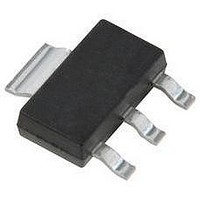
... Part Number Ordering Information Part Number No of Devices Container ADA-4789-TR1G 3000 ADA-4789-BLKG 100 SOT 89 Package Dimensions 11 13" Reel Anti-Static Bag Notes: 1. Dimensioning and tolerancing per ANSI.Y14.5M-1982 2. Controlling dimension: Milimeter convert to Inch are not necessary exact. 3. Dimension B1, 2 places. ...

Page 12

Device Orientation Tape Dimensions For product information and a complete list of distributors, please go to our web site: Avago, Avago Technologies, and the A logo are trademarks of Avago Technologies, Limited in the United States and other countries. Data ...

Related keywords