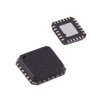
ADL5330ACPZ-REEL7 Analog Devices Inc, ADL5330ACPZ-REEL7 Datasheet - Page 12

ADL5330ACPZ-REEL7
Manufacturer Part Number
ADL5330ACPZ-REEL7
Description
IC AMP/ATTENUATOR RF VAR 24LFCSP
Manufacturer
Analog Devices Inc
Datasheet
1.ADL5330ACPZ-REEL7.pdf
(24 pages)
Specifications of ADL5330ACPZ-REEL7
Design Resources
Stable, Closed-Loop Automatic Power Control for RF Appls (CN0050)
Current - Supply
250mA
Frequency
10MHz ~ 3GHz
Gain
10dB
P1db
1.2dBm
Package / Case
24-VFQFN, 24-CSP Exposed Pad
Rf Type
Cellular, CDMA2000, W-CDMA, GSM
Test Frequency
2.7GHz
Voltage - Supply
4.75 V ~ 5.25 V
No. Of Amplifiers
1
No. Of Channels
1
Supply Voltage Range
4.75V To 5.25V
Amplifier Case Style
LFCSP
No. Of Pins
24
Operating Temperature Range
-40°C To +85°C
Termination Type
SMD
Lead Free Status / RoHS Status
Lead free / RoHS Compliant
Noise Figure
-
Lead Free Status / RoHS Status
Lead free / RoHS Compliant, Lead free / RoHS Compliant
Other names
ADL5330ACPZ-REEL7
ADL5330ACPZ-REEL7TR
ADL5330ACPZ-REEL7TR
Available stocks
Company
Part Number
Manufacturer
Quantity
Price
Company:
Part Number:
ADL5330ACPZ-REEL7
Manufacturer:
VISHAY
Quantity:
1 600
Part Number:
ADL5330ACPZ-REEL7
Manufacturer:
ADI/亚德诺
Quantity:
20 000
ADL5330
THEORY OF OPERATION
The ADL5330 is a high performance, voltage-controlled
variable gain amplifier/attenuator for use in applications with
frequencies up to 3 GHz. This device is intended to serve as an
output variable gain amplifier (OVGA) for applications where a
reasonably constant input level is available and the output level
adjusts over a wide range. One aspect of an OVGA is the output
metrics, IP3 and P1dB, decrease with decreasing gain.
The signal path is fully differential throughout the device in
order to provide the usual benefits of differential signaling,
including reduced radiation, reduced parasitic feedthrough, and
reduced susceptibility to common-mode interference with other
circuits. Figure 31 provides a simplified schematic of the
ADL5330.
A controlled input impedance of 50 Ω is achieved through a
combination of passive and active (feedback-derived)
termination techniques in an input Gm stage. The input
compression point of the Gm stage is 1 dBm to 3 dBm,
depending on the input frequency.
Note that the inputs of the Gm stage are internally biased to a
dc level, and dc blocking capacitors are generally needed on the
inputs to avoid upsetting operation of the device.
The currents from the Gm stage are then injected into a
balanced ladder attenuator at a deliberately diffused location
along the ladder, wherein the location of the centroid of the
injection region is dependent on the applied gain control
voltage. The steering of the current injection into the ladder is
accomplished by proprietary means to achieve linear-in-dB gain
control and low distortion.
INLO
INHI
Gm STAGE
Figure 31. Simplified Schematic
CONTROL
GAIN
TRANSIMPEDANCE
AMPLIFIER
OPHI
OPLO
Rev. A | Page 12 of 24
Linear-in-dB gain control is accomplished by the application of
a voltage in the range of 0 Vdc to 1.4 Vdc to the gain control pin,
with maximum gain occurring at the highest voltage.
The output of the ladder attenuator is passed into a fixed-gain
transimpedance amplifier (TZA) to provide gain and buffer the
ladder terminating impedance from load variations. The TZA
uses feedback to improve linearity and to provide controlled
50 Ω differential output impedance. The quiescent current of
the output amplifier is adaptive; it is slaved to the gain control
voltage to conserve power at times when the gain (and hence,
output power) are low.
The outputs of the ADL5330 require external dc bias to the
positive supply voltage. This bias is typically supplied through
external inductors. The outputs are best taken differentially to
avoid any common-mode noise that is present, but, if necessary,
can be taken single-ended from either output.
If only a single output is used, it is still necessary to provide
bias to the unused output pin, and it is advisable to arrange a
reasonably equivalent ac load on the unused output. Differential
output can be taken via a 1:1 balun into a 50 Ω environment. In
virtually all cases, it is necessary to use dc blocking in the
output signal path.
At high gain settings, the noise floor is set by the input stage, in
which case the noise figure (NF) of the device is essentially
independent of the gain setting. Below a certain gain setting,
however, the input stage noise that reaches the output of the
attenuator falls below the input-equivalent noise of the output
stage. In such a case, the output noise is dominated by the
output stage itself; therefore, the overall NF of the device gets
worse on a dB-per-dB basis, because the gain is reduced below
the critical value. Figure 9 through Figure 13 provide details of
this behavior.


