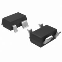
MGA-53543-BLKG Avago Technologies US Inc., MGA-53543-BLKG Datasheet - Page 6

MGA-53543-BLKG
Manufacturer Part Number
MGA-53543-BLKG
Description
IC AMP RFIC 1.9GHZ SOT-343
Manufacturer
Avago Technologies US Inc.
Type
General Purpose Amplifierr
Datasheet
1.MGA-53543-TR1G.pdf
(14 pages)
Specifications of MGA-53543-BLKG
P1db
18.6dBm
Noise Figure
1.5dB ~ 1.9dB
Package / Case
SC-70-4, SC-82-4, SOT-323-4, SOT-343
Current - Supply
40mA ~ 70mA
Frequency
50MHz ~ 6GHz
Gain
14dB ~ 17dB
Rf Type
Cellular, PCS, WLAN, WLL
Test Frequency
1.9GHz
Voltage - Supply
5V
Mounting Style
SMD/SMT
Technology
Linear Amplifier
Number Of Channels
1
Operating Frequency
6000 MHz
Operating Supply Voltage
5.5 V
Supply Current
70 mA @ 5 V
Maximum Power Dissipation
400 mW
Maximum Operating Temperature
+ 150 C
Manufacturer's Type
Linear Amplifier
Frequency (max)
6GHz
Operating Supply Voltage (max)
5.5V
Package Type
SOT-343
Mounting
Surface Mount
Pin Count
3 +Tab
Noise Figure (typ)
1.9@2400MHzdB
Lead Free Status / RoHS Status
Lead free / RoHS Compliant
Lead Free Status / RoHS Status
Lead free / RoHS Compliant, Lead free / RoHS Compliant
Other names
516-1946
MGA-53543-BLKG
MGA-53543-BLKG
Available stocks
Company
Part Number
Manufacturer
Quantity
Price
Company:
Part Number:
MGA-53543-BLKG
Manufacturer:
AMS
Quantity:
2 400
Company:
Part Number:
MGA-53543-BLKG
Manufacturer:
AVAGO
Quantity:
11 800
Part Number:
MGA-53543-BLKG
Manufacturer:
AVAGO/安华高
Quantity:
20 000
MGA-53543 Applications Information
Description
The MGA-53543 is a highly linear enhancement mode
PHEMT (Pseudomorphic High Electron Mobility Transistor)
amplifier with a frequency range extending from 450 MHz
to 6 GHz. This range makes the MGA-53543 ideal for both
Cellular and PCS basestation applications. With high IP3
and low noise figure, the MGA-53543 may be utilized as a
driver amplifier in a transmit chain or as a first or second
stage LNA in a receive chain or any other application
requiring high linearity.
The MGA-53543 operates from a +5 volt power supply and
draws a nominal current of 53.8 mA. The RFIC is contained
in a miniature SOT-343 (SC-70 4-lead) package to minimize
printed circuit board space. This package also offers good
thermal dissipation and RF characteristics.
Application Guidelines
For most applications, all that is required to operate the
MGA is to apply a DC bias of +5 volts and match the RF
input and output.
RF Input
The first step to achieve maximum linearity is to match
the input of MGA-53543 to one of the linearity values
listed on the data sheet. For example, at 1900 MHz the
MGA-53543 needs to see a complex impedance of 0.38
∠156° looking towards the source and an output imped-
ance of 0.05 ∠45° looking towards the load. This may be
accomplished by a conjugate match from the system
input impedance (typically 50Ω) to Γ
the location of these input and output Gammas (Γ
Γ
Figure 10. Matching for linearity at 1900 MHz.
6
Figure 1. Matching for Linearity at 1900 MHz.
L
) required for a high linearity.
Γ
S
Γ
L
S
*
. Figure 10 shows
S
and
RF Output
Few matching elements are required on the output of the
MGA-53543 to achieve good linearity because the output
Gamma (Γ
DC Bias
To bias the MGA-53543, a +5 volt supply is connected to
the output pin through an inductor, RFC, which isolates
the inband signal from the DC supply as shown in Figure
. Capacitor C3 serves as an RF bypass for inband signals
while C4 helps eliminate out of band low frequency sig-
nals. An optional resistor R1 may be added to de-Q any
resonance created between C3 and C4. Typically values
range from .Ω to 10Ω. A DC blocking capacitor, C, is
used at the output of the MMIC to isolate the supply volt-
age from succeeding circuits.
RF
Figure 11. Schematic diagram with bias connections.
Operating at Other Voltages
Operating this RFIC at voltages less than 5V will affect NF,
Gain, P1dB and IP3. Figure 1 below demonstrates the
affects of changing supply voltage at 1900 MHz.
Figure 12. Gain, NF and P1dB vs. supply voltage at 1900 MHz.
The affects of supply voltage on OIP3 and current at 1900
MHz are shown in Table 1. The MGA-53543 is internally
biased for optimal performance at a quiescent current
of 53.8 mA.
Figure 3. Gain, Noise Figure and P1dB vs.
Supply Voltage at 1900 MHz.
in
20
15
10
5
0
1
L1
C1
L
) is close to 50Ω.
2
SUPPLY VOLTAGE (V)
1
3
53
2
4
3
+5V
R1
4
RFC
C2
C3
C4
NF
Gain
P
1dB
RF
out
5


