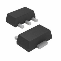
ADL5601ARKZ-R7 Analog Devices Inc, ADL5601ARKZ-R7 Datasheet

ADL5601ARKZ-R7
Specifications of ADL5601ARKZ-R7
ADL5601ARKZ-R7TR
Available stocks
Related parts for ADL5601ARKZ-R7
ADL5601ARKZ-R7 Summary of contents
Page 1
FEATURES Fixed gain Operation from 50 MHz to 4.0 GHz Highest dynamic range gain block Input/output internally matched to 50 Ω Integrated bias control circuit OIP3 of 43.0 dBm at 900 MHz P1dB of 19.0 dBm at ...
Page 2
ADL5601 TABLE OF CONTENTS Features .............................................................................................. 1 Functional Block Diagram .............................................................. 1 General Description ......................................................................... 1 Revision History ............................................................................... 2 Specifications ..................................................................................... 3 Typical Scattering Parameters (S-Parameters) ......................... 5 Absolute Maximum Ratings ............................................................ 7 ESD Caution .................................................................................. 7 Pin Configuration ...
Page 3
SPECIFICATIONS and T = 25°C, unless otherwise noted Table 1. Parameter OVERALL FUNCTION Frequency Range FREQUENCY = 50 MHz Gain Output 1 dB Compression Point (P1dB) Output Third-Order Intercept (OIP3) Second Harmonic Third Harmonic ...
Page 4
ADL5601 Parameter FREQUENCY = 900 MHz Gain vs. Frequency vs. Temperature vs. Supply Voltage Output 1 dB Compression Point (P1dB) Output Third-Order Intercept (OIP3) Second Harmonic Third Harmonic Noise Figure FREQUENCY = 2000 MHz Gain vs. Frequency vs. Temperature vs. ...
Page 5
Parameter POWER INTERFACE Supply Voltage ( Supply Current vs. Temperature Power Dissipation TYPICAL SCATTERING PARAMETERS (S-PARAMETERS 25°C, and the effects of the evaluation board have been deembedded up to the pins of ...
Page 6
ADL5601 S11 Frequency (MHz) Magnitude (dB) Angle (°) 2100 −10.11 +107.84 2150 −9.04 +96.61 2200 −8.12 +85.63 2250 −7.33 +74.68 2300 −6.66 +63.86 2350 −6.11 +53.33 2400 −5.65 +42.82 2450 −5.28 +32.51 2500 −5.00 +22.51 2550 −4.78 +12.49 2600 −4.64 ...
Page 7
ABSOLUTE MAXIMUM RATINGS Table 3. Parameter Supply Voltage Input Power (Referred to 50 Ω) Internal Power Dissipation (Paddle Soldered) θ (Junction to Air) JA θ (Junction to Paddle) JC Maximum Junction Temperature Lead Temperature (Soldering, 60 sec) Operating ...
Page 8
ADL5601 PIN CONFIGURATION AND FUNCTION DESCRIPTIONS Table 4. Pin Function Descriptions Pin No. Mnemonic Description 1 RFIN RF Input. This pin requires a dc blocking capacitor. 2 GND Ground. Connect this pin to a low impedance ground plane. 3 RFOUT ...
Page 9
TYPICAL PERFORMANCE CHARACTERISTICS 45 40 OIP3 P1dB GAIN 0.4 0.8 1.2 1.6 2.0 2.4 FREQUENCY (GHz) Figure 3. Noise Figure, Gain, P1dB, and OIP3 vs. Frequency 16.0 –40°C 15.5 15.0 ...
Page 10
ADL5601 –30 –40 –50 H2 –60 –70 H3 –80 –90 0 0.5 1.0 1.5 2.0 2.5 FREQUENCY (GHz) Figure 9. Single-Tone Harmonics vs. Frequency 14.5 14.7 14.9 15.1 15.3 ...
Page 11
BASIC CONNECTIONS The basic connections for operating the ADL5601 are shown in Figure 15. Recommended components are listed in Table 5. The input and output should be ac-coupled with appropriately sized capacitors (the device characterization was performed with 0.1 μF ...
Page 12
ADL5601 W-CDMA ACPR PERFORMANCE Figure 17 shows a plot of the adjacent channel power ratio (ACPR) vs. P for the ADL5601. The signal type used is a OUT single wideband code division multiple access (W-CDMA) carrier (Test Model 1, 64) ...
Page 13
EVALUATION BOARD Figure 18 shows the evaluation board layout, and Figure 19 shows the schematic for the ADL5601 evaluation board. The board is powered by a single 5 V supply. The components used on the board are listed in Table ...
Page 14
... ADL5601 OUTLINE DIMENSIONS 4.25 3.94 1.50 TYP ORDERING GUIDE Model Temperature Range 1 ADL5601ARKZ-R7 −40°C to +85°C 1 ADL5601-EVALZ RoHS Compliant Part. * 1.75 1.55 (2) 2.60 2. 1.20 0.75 3.00 TYP 2.29 2.14 4.60 4.40 0.44 0.35 END VIEW * 0.56 * 0.52 0.36 0.32 * COMPLIANT TO JEDEC STANDARDS TO-243 WITH EXCEPTION TO DIMENSIONS INDICATED BY AN ASTERISK ...
Page 15
NOTES Rev Page ADL5601 ...
Page 16
ADL5601 NOTES ©2009 Analog Devices, Inc. All rights reserved. Trademarks and registered trademarks are the property of their respective owners. D08219-0-9/09(0) Rev Page ...


