SKY65111-348LF Skyworks Solutions Inc, SKY65111-348LF Datasheet - Page 13
SKY65111-348LF
Manufacturer Part Number
SKY65111-348LF
Description
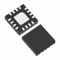
IC AMP INGAP 600-110MHZ 12-QFN
Manufacturer
Skyworks Solutions Inc
Datasheet
1.SKY65111-348LF.pdf
(16 pages)
Specifications of SKY65111-348LF
Gain
40dB
Rf Type
ISM
Current - Supply
250mA
Frequency
600MHz ~ 1.1GHz
P1db
29.5dBm
Package / Case
12-QFN
Test Frequency
902MHz ~ 928MHz
Voltage - Supply
3.5V
Frequency Range
800MHz To 1.1GHz
Supply Current
5mA
Supply Voltage Range
2.5V To 5V
Rf Ic Case Style
QFN
No. Of Pins
12
Operating Temperature Range
-40°C To +85°C
Package
RoHS Compliant
Lead Free Status / RoHS Status
Lead free / RoHS Compliant
Noise Figure
-
Lead Free Status / RoHS Status
Lead free / RoHS Compliant
Other names
863-1071-2
Available stocks
Company
Part Number
Manufacturer
Quantity
Price
Company:

Part Number:
SKY65111-348LF
Manufacturer:
SKYWORKS
Quantity:
1 200
Company:
Part Number:
SKY65111-348LF
Manufacturer:
Skyworks Solutions Inc
Quantity:
28 918
Part Number:
SKY65111-348LF
Manufacturer:
SKYWORKS/思佳讯
Quantity:
20 000


Application Circuit Notes
Ground, (Pins 1, 3, 8, 14). Attach all ground pins to the RF
ground plane with the largest diameter and lowest inductance via
that the layout will allow. Multiple small vias are also acceptable
and will work well under the device if solder migration is an
issue. It is extremely important that the device paddle be suffi-
ciently grounded for both thermal and stability reasons. Please
refer to the enclosed Package Footprint.
RF input (Pin 2). A lumped element matching structure for good
in-band return loss has been realized on the RF input, Pin 2. This
structure is comprised of a DC blocking capacitor (C1), low pass
LC filter (L1, C1) and at the device input, a series capacitor (C25).
This combination of devices will yield a return loss better than -
11 dB over the entire 800–1100 MHz band of interest. The
placement of C1 is not critical; it can be moved as close to L1,
C2 and C25 as desired. C25 should be placed as close to the
device pin as possible to replicate performance as measured on
the applications board.
V
stage in the SKY65111. Multiple bypass capacitors, C3-C5, C17
and a series inductor, L2, have been utilized to ensure stability
both in and out of the useable bandwidth of the device. The
length of transmission line between L2 and Pin 4 is not critical;
L2 can be placed as close to the pin as possible if desired.
However, placement of L2 farther away from Pin 4 than shown
on the Applications Circuit is not recommended. C3 should also
be placed in the approximate location shown on the Applications
Circuit, but placement is not critical.
V
stages 1 and 2. Nominal operating range is between 2.6 V
2.8 V
V
standby mode.
V
stage 3. Nominal operating range is between 2.6 V
2.8 V
A 100 pF capacitor (C19) may be used for bypassing at high
frequencies. The value of this capacitor may also be made large,
greater than 1000 pF, if longer response time is acceptable.
V
standby status.
NOTE: In most applications V
APC
APC
CC
APC
APC
1 (Pin 4). V
1 may also be set to 0 V
2 may also be set to 0 V
1 (Pin 5). V
2 (Pin 6). V
DC
DC
, with 3 V
, with 3 V
together and biased from the same control voltage. V
and V
desired.
APC
CC
2 may also be split if independent control is
APC
APC
DC
DC
1 is the collector bias for the first amplifier
Skyworks Solutions, Inc. • Phone [781] 376-3000 • Fax [781] 376-3100 • sales@skyworksinc.com • www.skyworksinc.com
200428 Rev. E • Skyworks Proprietary Information. • Products and product information are subject to change without notice. • February 12, 2007
1 is the bias control voltage input for amplifier
producing the minimum attenuation point.
2 is the bias control voltage for amplifier
producing the minimum attenuation point.
DC
DC
APC
, to force stages 1 and 2 into
, to place amplifier stage 3 into
1 and V
APC
2 pins are directly tied
DC
and
DC
APC
and
1
V
stages 2 and 3. V
range as V
V
as close to the device pin as possible.
RF
the stage 3 collectors. Bias is applied to the RF output through a
length of transmission line that is approximately 827 mils (21
mm) long. Capacitors C11-C14 provide proper RF bypassing and
should be placed as shown in the Applications Circuit. Output
matching for optimal power gain is accomplished with capacitors
C15 and C16. Spacing between these capacitors with respect to
the RF output and each other is critical and is shown on the
Component Placement Diagram. Special care must be taken
when placing these devices; their locations should not deviate
significantly from the locations as shown. If these capacitors are
not located properly, large decreases in output power and effi-
ciency will occur.
Pin 13. Pin 13 has no connection and should be left open circuit.
V
amplifier stage in the SKY65111. Multiple bypass capacitors,
C8-C10 have been utilized to ensure stability both in and out of
the useable bandwidth of the device. Capacitor C7 is not popu-
lated with the normal tuning configuration described above.
REF
REF
CC
OUT
2 (Pins 15-16). V
is accomplished with C22 and C23 which should be placed
(Pin 7). V
, V
CC
CC
3 (Pins 9-12). RF
, with a nominal voltage of 3.5 V
REF
REF
is the bias reference voltage for amplifier
should be operated over the same voltage
CC
2 is the collector bias input for the second
OUT
and V
DATA SHEET • SKY65111-348LF
CC
3 are the biasing input of
DC
. Bypassing of
13
Related parts for SKY65111-348LF
Image
Part Number
Description
Manufacturer
Datasheet
Request
R

Part Number:
Description:
Manufacturer:
Skyworks Solutions Inc
Datasheet:
Part Number:
Description:
Manufacturer:
Skyworks Solutions Inc
Datasheet:
Part Number:
Description:
Manufacturer:
Skyworks Solutions Inc
Datasheet:
Part Number:
Description:
Manufacturer:
Skyworks Solutions Inc
Datasheet:
Part Number:
Description:
Manufacturer:
Skyworks Solutions Inc
Datasheet: