ALM-1412-TR1G Avago Technologies US Inc., ALM-1412-TR1G Datasheet - Page 6
ALM-1412-TR1G
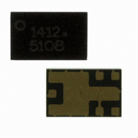
Manufacturer Part Number
ALM-1412-TR1G
Description
IC AMP GPS LNA 12-MCOB
Manufacturer
Avago Technologies US Inc.
Type
GPS Filter-LNA-Filter Front-End Moduler
Datasheet
1.ALM-1412-TR1G.pdf
(17 pages)
Specifications of ALM-1412-TR1G
P1db
4.5dBm
Noise Figure
0.82dB
Package / Case
12-MCOB
Current - Supply
9.8mA
Frequency
1.575GHz
Gain
12.2dB
Rf Type
GPS
Test Frequency
1.575GHz
Voltage - Supply
1 V ~ 3.6 V
Mounting Style
SMD/SMT
Operating Frequency
1.575 GHz
Operating Supply Voltage
1 V to 3.6 V
Supply Current
20 mA
Maximum Power Dissipation
72 mW
Maximum Operating Temperature
+ 85 C
Minimum Operating Temperature
- 40 C
Frequency Rf
1.575GHz
Noise Figure Typ
0.82dB
Power Dissipation Pd
72mW
Supply Voltage Range
1V To 3.6V
Filter Terminals
SMD
Supply Voltage Max
3.6V
Rohs Compliant
Yes
Frequency Range
1.575GHz
No. Of Pins
12
Operating Temperature Range
-40°C To +85°C
Lead Free Status / RoHS Status
Lead free / RoHS Compliant
Lead Free Status / RoHS Status
Lead free / RoHS Compliant, Lead free / RoHS Compliant
Other names
516-1998-2
Available stocks
Company
Part Number
Manufacturer
Quantity
Price
Company:

Part Number:
ALM-1412-TR1G
Manufacturer:
AVAGO
Quantity:
17 460
Company:
Part Number:
ALM-1412-TR1G
Manufacturer:
AVAGO
Quantity:
3 200
Part Number:
ALM-1412-TR1G
Manufacturer:
AVAGO/安华高
Quantity:
20 000


Figure 7. Demoboard and application schematic diagram
Notes:
x The demoboard of Figure 6 is Rogers® RO4350 with typical Dk=3.48 (@10GHz).
x L3 and the module’s internal input pre-match form the input matching network. The RFin pin, pin 1, is directly connected to a shunt inductor
x This circuit demonstrates that very low noise figure is obtainable with standard 0402 chip inductors instead of high-Q wirewound inductors.
x C2 and L2 form a matching network at the output of the LNA stage, which can be tuned to optimize gain and return loss. For example, higher
x L1 is a choke which isolates the demoboard from external disturbances during measurement. It is not needed in actual application. Likewise,
x R1 is a stability-enhancing resistor.
x C9 is a DC-blocking capacitor. It is also not required in actual operation.
x Bias control is achieved by either varying the SD voltage (Vsd) with/without R2, or fixing the SD voltage to Vdd and adjusting R2 for the desired
x For low-voltage operation such as Vdd = 1.5 V or 1.0 V, R2 may be omitted and SD (Vsd) connected directly to Vdd.
x The grounding regime for the ALM-1412 is critical to achieving the PCS- and Cell-Band Rejections shown in Figure 9. Please refer to the PCB
6
that is grounded. The RF output filter blocks DC.
gain can be obtained by increasing the value of C2 but at the expense of stability. Changing the value of L2 can improve the PCS rejection,
but impacts output return loss.
C1 and C3 mitigate the effect of external noise pickup on the Vdd and SD lines respectively. These components are not required in actual
operation.
current. Typical value for R2 is 10k Ohms for 8 mA total current at Vdd = 2.85 V and Vsd = +2.60 V. For applications where it is more appropriate
to have SD (Vsd) connected to Vdd, a 12 k Ohms resistor value for R2 is suggested (where Vdd = 2.85 V).
Land Patterns section of this document for the exact locations of the grounding vias.
50-Ohms TL
2, 4, 5, 6, 7, 9, 10, 11
GND
1, 4
L3
1
2
3
SD
MATCH
INPUT
Vdd
C2
R2
R1
L2
3
C3
12
L1
FILTER
C1
8
C9
MODULE OUTLINE
Z1
50-Ohms TL
Related parts for ALM-1412-TR1G
Image
Part Number
Description
Manufacturer
Datasheet
Request
R

Part Number:
Description:
IC AMP LNA GPS W/FILTER 12MCOB
Manufacturer:
Avago Technologies US Inc.
Datasheet:

Part Number:
Description:
RF Amplifier GPS LNA with Filter
Manufacturer:
Avago Technologies US Inc.

Part Number:
Description:
IC AMP LNA GPS FRONT-END 2.5X3MM
Manufacturer:
Avago Technologies US Inc.
Datasheet:

Part Number:
Description:
GPS Filter/LNA/Filter
Manufacturer:
Avago Technologies US Inc.
Datasheet:
Part Number:
Description:
Margosa Halogen Free
Manufacturer:
Avago Technologies US Inc.
Datasheet:
Part Number:
Description:
Margosa Halogen Free
Manufacturer:
Avago Technologies US Inc.
Datasheet:
Part Number:
Description:
Margosa Halogen Free
Manufacturer:
Avago Technologies US Inc.
Datasheet:
Part Number:
Description:
IC,Microwave/Millimeter Wave Amplifier,SINGLE,GAAS,LLCC,22PIN,PLASTIC
Manufacturer:
Avago Technologies US Inc.
Datasheet:
Part Number:
Description:
IC,Microwave/Millimeter Wave Amplifier,SINGLE,GAAS,LLCC,22PIN,PLASTIC
Manufacturer:
Avago Technologies US Inc.
Datasheet:
Part Number:
Description:
IC,Microwave/Millimeter Wave Amplifier,SINGLE,GAAS,LLCC,22PIN,PLASTIC
Manufacturer:
Avago Technologies US Inc.
Datasheet:
Part Number:
Description:
Dual Band WLAN LNA
Manufacturer:
Avago Technologies US Inc.
Datasheet:
Part Number:
Description:
IC,Microwave/Millimeter Wave Amplifier,SINGLE,GAAS,LLCC,6PIN,PLASTIC
Manufacturer:
Avago Technologies US Inc.
Datasheet:
Part Number:
Description:
IC,Microwave/Millimeter Wave Amplifier,SINGLE,GAAS,LLCC,6PIN,PLASTIC
Manufacturer:
Avago Technologies US Inc.
Datasheet:
Part Number:
Description:
IC,Microwave/Millimeter Wave Amplifier,SINGLE,GAAS,MODULE,22PIN,PLASTIC
Manufacturer:
Avago Technologies US Inc.
Datasheet:
Part Number:
Description:
IC,Microwave/Millimeter Wave Amplifier,DUAL,MODULE,22PIN,PLASTIC
Manufacturer:
Avago Technologies US Inc.
Datasheet: