UPC2710TB-EVAL CEL, UPC2710TB-EVAL Datasheet
UPC2710TB-EVAL
Specifications of UPC2710TB-EVAL


Related parts for UPC2710TB-EVAL


UPC2710TB-EVAL Summary of contents
Page 1
To our customers, Old Company Name in Catalogs and Other Documents st On April 1 , 2010, NEC Electronics Corporation merged with Renesas Technology Corporation, and Renesas Electronics Corporation took over all the business of both companies. Therefore, although the ...
Page 2
All information included in this document is current as of the date this document is issued. Such information, however, is subject to change without any prior notice. Before purchasing or using any Renesas Electronics products listed herein, please confirm ...
Page 3
... MEDIUM OUTPUT POWER AMPLIFIER DESCRIPTION The µ PC2710TB is a silicon monolithic integrated circuit designed as PA driver for 900 MHz band cellular telephone tuners. This IC is packaged in super minimold package which is smaller than conventional minimold. This IC is manufactured using NEC’s 20 GHz f nitride passivation film and gold electrodes ...
Page 4
PIN CONNECTIONS (Top View +25° ° ° ° PRODUCT LINE- O(sat) Part No. (GHz) (dBm) µ PC2708T 2.9 +10.0 µ PC2708TB µ PC2709T 2.3 +11.5 µ ...
Page 5
... SYSTEM APPLICATION EXAMPLE EXAMPLE OF 900 MHz BAND DIGITAL CELLULER TELEPHONE RX SW Driver TX PA µ PC2710TB DEMOD. PLL PLL 0 ° φ 90 ° Data Sheet P13443EJ3V0DS µ µ µ µ PC2710TB ...
Page 6
... Pin Function and Applications Note Signal input pin. A internal matching circuit, configured with resistors, enables 50 Ω connection over a wide band. A multi-feedback circuit is designed to cancel the deviations of h and FE resistance. This pin must be coupled to signal source with capacitor for DC cut. – Ground pin. This pin should ...
Page 7
ABSOLUTE MAXIMUM RATINGS Parameter Symbol Supply Voltage V CC Total Circuit Current I CC Power Dissipation P D Operating Ambient Temperature T A Storage Temperature T stg Input Power P in RECOMMENDED OPERATING RANGE Parameter Symbol Supply Voltage V CC ...
Page 8
TEST CIRCUIT 50 Ω 000 pF COMPONENTS OF TEST CIRCUIT FOR MEASURING ELECTRICAL CHARACTERISTICS Type Value Bias Tee 1 000 Capacitor 1 000 Bias Tee 1 000 ...
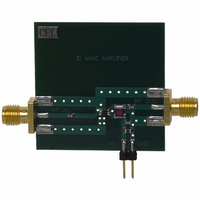
Page 9
ILLUSTRATION OF THE TEST CIRCUIT ASSEMBLED ON EVALUATION BOARD Top View IN Mounting Direction Notes COMPONENT LIST 1. Value 000 300 nH 4. For more information on the use of this IC, refer to ...
Page 10
TYPICAL CHARACTERISTICS (Unless otherwise specified, T CIRCUIT CURRENT vs. SUPPLY VOLTAGE 40 No signal Supply Voltage V NOISE FIGURE, POWER GAIN vs. FREQUENCY 35 4 5.5 V ...
Page 11
OUTPUT POWER vs. INPUT POWER + 5 0.5 GHz + −5 −10 −15 −35 −30 −25 −20 −15 −10 −5 −40 ...
Page 12
C, V S-PARAMETERS ( -FREQUENCY FREQUENCY 5.0 V) out 0.1 GHz 3.0 GHz 2.0 GHz 1.0 GHz 3.0 GHz 0.1 GHz 2.0 GHz 1.0 ...
Page 13
TYPICAL S-PARAMETER VALUES ( 5 out CC FREQUENCY S 11 MHz MAG. ANG. 100.0000 0.306 2.5 200.0000 0.324 5.2 300.0000 0.356 5.3 400.0000 0.400 2.5 −3.3 500.0000 0.439 −10.2 600.0000 ...
Page 14
PACKAGE DIMENSIONS 6-PIN SUPER MINIMOLD (UNIT: mm) 12 2.1±0.1 1.25±0.1 0.1 MIN. Data Sheet P13443EJ3V0DS µ µ µ µ PC2710TB ...
Page 15
NOTES ON CORRECT USE (1) Observe precautions for handling because of electro-static sensitive devices. (2) Form a ground pattern as widely as possible to minimize ground impedance (to prevent undesired oscillation). All the ground pins must be connected together with ...
Page 16
Data Sheet P13443EJ3V0DS µ µ µ µ PC2710TB ...
Page 17
Data Sheet P13443EJ3V0DS µ µ µ µ PC2710TB 15 ...
Page 18
NESAT (NEC Silicon Advanced Technology trademark of NEC Corporation. • The information in this document is current as of January, 2001. The information is subject to change without notice. For actual design-in, refer to the latest publications of ...