EVAL-ADM1062LFEBZ Analog Devices Inc, EVAL-ADM1062LFEBZ Datasheet - Page 6
EVAL-ADM1062LFEBZ
Manufacturer Part Number
EVAL-ADM1062LFEBZ
Description
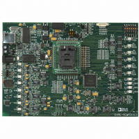
BOARD EVALUATION FOR ADM1062LF
Manufacturer
Analog Devices Inc
Datasheet
1.EVAL-ADM1062LFEB.pdf
(36 pages)
Specifications of EVAL-ADM1062LFEBZ
Main Purpose
Power Management, Power Supply Supervisor/Tracker/Sequencer
Embedded
No
Utilized Ic / Part
ADM1062
Primary Attributes
10 Inputs, 10 Outputs (6 can be FET Drivers)
Secondary Attributes
Graphical User Interface
Lead Free Status / RoHS Status
Lead free / RoHS Compliant


ADM1062
Parameter
DIGITAL INPUTS (VXx, A0, A1)
SERIAL BUS DIGITAL INPUTS (SDA, SCL)
SERIAL BUS TIMING
SEQUENCING ENGINE TIMING
1
2
3
At least one of the VH, VPx pins must be ≥3.0 V to maintain the device supply on VDDCAP.
All temperature sensor measurements are taken with round-robin loop enabled and at least one other voltage input being measured.
Specification is not production tested but is supported by characterization data at initial product release.
Three-State Output Leakage Current
Oscillator Frequency
Input High Voltage, V
Input Low Voltage, V
Input High Current, I
Input Low Current, I
Input Capacitance
Programmable Pull-Down Current, I
Input High Voltage, V
Input Low Voltage, V
Output Low Voltage, V
Clock Frequency, f
Bus Free Time, t
Start Setup Time, t
Stop Setup Time, t
Start Hold Time, t
SCL Low Time, t
SCL High Time, t
SCL, SDA Rise Time, t
SCL, SDA Fall Time, t
Data Setup Time, t
Data Hold Time, t
Input Low Current, I
State Change Time
I
I
R
I
OL
SINK
SOURCE
PULL-UP
3
3
(VPx)
3
BUF
LOW
HIGH
HD;STA
HD;DAT
SCLK
SU;STO
SU;DAT
SU;STA
IL
IL
F
IL
IH
IL
R
IH
IH
OL
3
PULL-DOWN
Min
16
90
2.0
−1
2.0
4.7
4.7
4
4
4.7
4
250
5
Typ
20
100
5
20
10
Rev. B | Page 6 of 36
Max
20
60
29
2
10
110
0.8
1
0.8
0.4
400
1000
300
1
Unit
mA
mA
kΩ
mA
μA
kHz
V
V
μA
μA
pF
μA
V
V
V
kHz
μs
μs
μs
μs
μs
μs
μs
μs
ns
ns
μA
μs
Test Conditions/Comments
Maximum sink current per PDOx pin
Maximum total sink for all PDOx pins
Internal pull-up
Current load on any VPx pull-ups, that is, total source
current available through any number of PDOx pull-up
switches configured onto any one VPx pin
V
All on-chip time delays derived from this clock
Maximum V
Maximum V
V
V
VDDCAP = 4.75 V T
I
V
OUT
PDO
IN
IN
IN
= 5.5 V
= 0 V
= 0
= −3.0 mA
= 14.4 V
IN
IN
= 5.5 V
= 5.5 V
A
= 25°C if known logic state is required
Related parts for EVAL-ADM1062LFEBZ
Image
Part Number
Description
Manufacturer
Datasheet
Request
R

Part Number:
Description:
IC, ADJ LDO REG, 1.5V TO 5V 250mA MSOP-8
Manufacturer:
Vishay
Datasheet:

Part Number:
Description:
IC, ADJ LDO REG, 1.5V TO 5V 0.6A 8-TSSOP
Manufacturer:
Vishay
Datasheet:
Part Number:
Description:
IC, ADJ LDO REG, 1.5V TO 5V 250mA MSOP-8
Manufacturer:
Vishay
Datasheet:

Part Number:
Description:
IC ADJ LDO REG 1.5V TO 5V 150mA 5-SOT-23
Manufacturer:
Vishay
Datasheet:

Part Number:
Description:
BOARD EVAL AS1324-AD
Manufacturer:
austriamicrosystems
Datasheet:
Part Number:
Description:
IC, ADJ LDO REG, 1.5V TO 5V 0.6A 8-TSSOP
Manufacturer:
Vishay
Datasheet:

Part Number:
Description:
IC, ADJ LDO REG, 1.5V TO 5V, 0.3A, MSOP8
Manufacturer:
Vishay
Datasheet:
Part Number:
Description:
IC, ADJ LDO REG, 1.5V TO 5V, 0.3A, MSOP8
Manufacturer:
Vishay
Datasheet:
Part Number:
Description:
IC, ADJ LDO REG 1.215V TO 5V 0.3A MSOP-8
Manufacturer:
Vishay
Datasheet:
Part Number:
Description:
IC, ADJ LDO REG 1.215V TO 5V 0.3A MSOP-8
Manufacturer:
Vishay
Datasheet:

Part Number:
Description:
±1.7g Dual-Axis IMEMS Accelerometer Evaluation Board
Manufacturer:
Analog Devices Inc
Datasheet:

Part Number:
Description:
IC MULTIPLIER ANALOG 8-SOIC T/R
Manufacturer:
Analog Devices Inc
Datasheet:

Part Number:
Description:
IC ANALOG MULTIPLIER 8-DIP
Manufacturer:
Analog Devices Inc
Datasheet:
Part Number:
Description:
IC ANALOG MULTIPLIER 8-SOIC
Manufacturer:
Analog Devices Inc
Datasheet:
Part Number:
Description:
IC ANALOG MULTIPLIER 8-DIP
Manufacturer:
Analog Devices Inc
Datasheet: