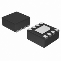
NCP5359AMNR2G ON Semiconductor, NCP5359AMNR2G Datasheet - Page 7

NCP5359AMNR2G
Manufacturer Part Number
NCP5359AMNR2G
Description
IC MOSFET GATE DVR DUAL 8-DFN
Manufacturer
ON Semiconductor
Type
High Side/Low Sider
Datasheet
1.NCP5359AMNTBG.pdf
(9 pages)
Specifications of NCP5359AMNR2G
Configuration
High and Low Side, Synchronous
Input Type
PWM
Delay Time
10.0ns
Number Of Configurations
1
Number Of Outputs
2
High Side Voltage - Max (bootstrap)
30V
Voltage - Supply
10 V ~ 13.2 V
Operating Temperature
0°C ~ 85°C
Mounting Type
Surface Mount
Package / Case
8-VFDFN Exposed Pad
Product
MOSFET Gate Drivers
Propagation Delay Time
25 ns
Supply Voltage (max)
15 V
Supply Voltage (min)
- 0.3 V
Maximum Operating Temperature
+ 150 C
Mounting Style
SMD/SMT
Minimum Operating Temperature
0 C
Output Voltage
35 V
Lead Free Status / RoHS Status
Lead free / RoHS Compliant
Current - Peak
-
Lead Free Status / Rohs Status
Lead free / RoHS Compliant
Available stocks
Company
Part Number
Manufacturer
Quantity
Price
Company:
Part Number:
NCP5359AMNR2G
Manufacturer:
FREESCALE
Quantity:
101
Part Number:
NCP5359AMNR2G
Manufacturer:
ON/安森美
Quantity:
20 000
driver designed for driving two N−channel MOSFETs in a
synchronous buck converter topology. This driver is
compatible with the NCP3418B gate drive. This gate drives
operation is similar with the NCP3418B, but has two
additional new features: Bidirection fault detection and
multilevel PWM input. When the gate driver works with
ON Semiconductor’s NCP5392 controller, it can provide a
difference output logic status through multi−level PWM
input. For this new feature, higher efficiency can be
provided. For the bidirection fault detection function, it is
used to provide a driver state information to other gate
drivers and controller in a multiphase buck converter. e.g
overvoltage protection (OVP) function at startup, thermal
shutdown and undervoltage lockout (UVLO). This feature
can provide an additional protection function for the
multi−phase system when the fault condition occurs in one
channel. With this additional feature, converter overall
system will be more reliable and safe.
Enable Pin
MOSFET. This pin is controlled by internal or external
signal. There are three conditions will be triggered:
pull low. In this case, the drive output DRVH and DRVL will
be forced low, until the fault mode remove then restart
automatic.
Undervoltage Lockout
during startup. The PWM signals will control the gate status
when V
below the threshold, the output gate will be forced low until
input voltage V
The NCP5359A gate driver is a single phase MOSFET
The bidirection enable pin is connected with an open drain
When the internal fault has been detected, EN pin will be
The DRVH and DRVL are held low until V
1. The voltage at SWN pin is higher than preset
2. The controller hits the UVLO at V
3. The controller hits the thermal shutdown.
voltage at power startup.
CC
threshold is exceeded. If V
CC
rises above the startup threshold.
CC
decreases to 3.2 V
CC
CC
APPLICATION INFORMATION
pin.
reaches 9 V
http://onsemi.com
7
Power ON reset
abnormal status driving the startup condition. When the
initial soft−start voltage is higher than 3.2 V, the gate driver
will monitor the switching node SW pin. If SW pin high than
1.9 V, bottom gate will be force to high for discharge the
output capacitor. The fault mode will be latch and EN pin
will force to be low, unless the driver is recycle. When input
voltage is higher than 9 V, the gate driver will normal
operation, top gate driver DRVH and bottom gate driver will
follow the PWM signal decode to a status.
Adaptive Nonoverlap
shoot through damage the power MOSFETs. When the
PWM signal pull high, DRVL will go low after a
propagation delay, the controller will monitors the switching
node (SWN) pin voltage and the gate voltage of the
MOSFET to know the status of the MOSFET. When the low
side MOSFET status is off an internal timer will delay turn
on of the high–side MOSFET. When the PWM pull low, gate
DRVH will go low after the propagation delay (tpd DRVH).
The time to turn off the high side MOSFET is depending on
the total gate charge of the high−side MOSFET. A timer will
be triggered once the high side MOSFET is turn off to delay
the turn on the low−side MOSFET.
Layout Guidelines
converter. Bootstrap capacitor and V
critical items, it should be placed as close as to the driver IC.
Another item is using a GND plane. Ground plane can
provide a good return path for gate drives for reducing the
ground noise. Therefore GND pin should be directly
connected to the ground plane and close to the low−side
MOSFET source pin. Also, the gate drive trace should be
considered. The gate drives has a high di/dt when switching,
therefore a minimized gate drives trace can reduce the di/dv,
raise and fall time for reduce the switching loss.
Power on reset feature is used to protect a gate driver avoid
The nonoverlap dead time control is used to avoid the
Layout is very important thing for design a DC−DC
CC
capacitor are most


