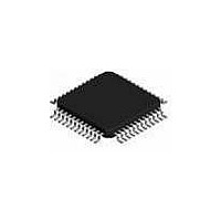
ST16C550IQ48-F Exar Corporation, ST16C550IQ48-F Datasheet - Page 5

ST16C550IQ48-F
Manufacturer Part Number
ST16C550IQ48-F
Description
IC UART FIFO 16B SGL 48TQFP
Manufacturer
Exar Corporation
Type
UART with 16-byte FIFOsr
Datasheet
1.ST16C550CJ44-F.pdf
(35 pages)
Specifications of ST16C550IQ48-F
Number Of Channels
1, UART
Package / Case
48-TQFP
Features
*
Fifo's
16 Byte
Voltage - Supply
2.97 V ~ 5.5 V
With False Start Bit Detection
Yes
With Modem Control
Yes
With Cmos
Yes
Mounting Type
Surface Mount
Data Rate
1.5 Mbps
Supply Voltage (max)
5.5 V
Supply Voltage (min)
2.97 V
Supply Current
3 mA
Maximum Operating Temperature
+ 85 C
Minimum Operating Temperature
- 40 C
Mounting Style
SMD/SMT
Operating Supply Voltage
3.3 V, 5 V
No. Of Channels
1
Supply Voltage Range
2.97V To 5.5V
Operating Temperature Range
-40°C To +85°C
Digital Ic Case Style
TQFP
No. Of Pins
48
Filter Terminals
SMD
Rohs Compliant
Yes
Lead Free Status / RoHS Status
Lead free / RoHS Compliant
Lead Free Status / RoHS Status
Lead free / RoHS Compliant, Lead free / RoHS Compliant
Other names
1016-1262
Available stocks
Company
Part Number
Manufacturer
Quantity
Price
Company:
Part Number:
ST16C550IQ48-F
Manufacturer:
EXAR
Quantity:
3 000
Company:
Part Number:
ST16C550IQ48-F
Manufacturer:
EXAR21
Quantity:
410
Company:
Part Number:
ST16C550IQ48-F
Manufacturer:
Exar Corporation
Quantity:
10 000
SYMBOL DESCRIPTION
-IOR
-IOW
INT
-RXRDY
-TXRDY
-BAUDOUT
Symbol
Rev. 5.01
40
21
18
30
29
24
15
Pin
44
24
20
33
27
17
32
19
48
16
30
29
23
12
Signal
type
O
O
O
O
I
I
Read data strobe (active low strobe). A logic 0 on this pin
transfers the contents of the ST16C550 data bus to the CPU.
Connect to logic 1 when using IOR.
Write data strobe (active low strobe). A logic 0 on this pin
transfers the contents of the CPU data bus to the addressed
internal register. Connect to logic 1 when using IOW.
Interrupt Request (active high). Interrupts are enabled in the
interrupt enable register (IER), and when an interrupt con-
dition exists. Interrupt conditions include: receiver errors,
available receiver buffer data, transmit buffer empty, or
when a modem status flag is detected.
Receive Ready. When operating in the FIFO mode, one of
two types of DMA signaling can be selected using the FIFO
control register bit-3. When operating in the ST16C450
mode, only DMA mode “0” is allowed. Mode “0” supports
single transfer DMA in which a transfer is made between
CPU bus cycles. Mode “1” supports multi-transfer DMA in
which multiple transfers are made continuously until the
receiver FIFO has been emptied. In DMA mode “0” -RXRDY
is low, when there is at least one character in the receiver
FIFO or receive holding register. In DMA mode “1”, -RXRDY
is low, when the trigger level or the time-out has been
reached.
Transmit Ready. When operating in the FIFO mode, one of
two types of DMA signaling can be selected using the FIFO
control register bit-3. When operating in the ST16C450
mode, only DMA mode “0” is allowed. Mode “0” supports
single transfer DMA in which a transfer is made between
CPU bus cycles. Mode “1” supports multi-transfer DMA in
which multiple transfers are made continuously until the
transmit FIFO has been filled.
Baud Rate Generator Output. This pin provides the 16X
clock of the selected data rate from the baud rate generator.
The RCLK pin must be connected externally to -BAUDOUT
when the receiver is operating at the same data rate.
5
Pin Description
ST16C550


