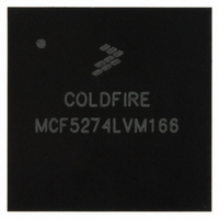
MCF5274LVM166 Freescale Semiconductor, MCF5274LVM166 Datasheet - Page 24

MCF5274LVM166
Manufacturer Part Number
MCF5274LVM166
Description
IC MPU 32BIT COLDF 196-MAPBGA
Manufacturer
Freescale Semiconductor
Series
MCF527xr
Datasheet
1.MCF5274LVM166J.pdf
(44 pages)
Specifications of MCF5274LVM166
Core Processor
Coldfire V2
Core Size
32-Bit
Speed
166MHz
Connectivity
EBI/EMI, Ethernet, I²C, SPI, UART/USART, USB
Peripherals
DMA, WDT
Number Of I /o
61
Program Memory Type
ROMless
Ram Size
64K x 8
Voltage - Supply (vcc/vdd)
1.4 V ~ 1.6 V
Oscillator Type
External
Operating Temperature
0°C ~ 70°C
Package / Case
196-MAPBGA
Embedded Interface Type
I2C, SPI, USB, UART
Digital Ic Case Style
BGA
No. Of Pins
196
Operating Temperature Range
0°C To +70°C
Frequency Typ
166MHz
Rohs Compliant
Yes
Family Name
MCF5xxx
Device Core
ColdFire
Device Core Size
32b
Frequency (max)
166MHz
Instruction Set Architecture
RISC
Operating Supply Voltage (max)
1.6V
Operating Supply Voltage (min)
1.4V
Operating Temp Range
0C to 70C
Operating Temperature Classification
Commercial
Mounting
Surface Mount
Pin Count
196
Package Type
MA-BGA
Lead Free Status / RoHS Status
Lead free / RoHS Compliant
Eeprom Size
-
Program Memory Size
-
Data Converters
-
Lead Free Status / Rohs Status
Compliant
Available stocks
Company
Part Number
Manufacturer
Quantity
Price
Company:
Part Number:
MCF5274LVM166
Manufacturer:
FREESCALE
Quantity:
201
Company:
Part Number:
MCF5274LVM166
Manufacturer:
Freescale Semiconductor
Quantity:
10 000
Company:
Part Number:
MCF5274LVM166J
Manufacturer:
Freescale Semiconductor
Quantity:
10 000
Electrical Characteristics
8.6
Table 12
24
1
2
3
B0
B1a
B1b
B2a
B2b
B4
B5
Name
Timing specifications have been indicated taking into account the full drive strength for the pads.
TEA and TA pins are being referred to as control inputs.
4
5
6
7
8
9
10
11
12
13
14
15
16
Refer to figure A-19.
Self clocked mode frequency is the frequency that the PLL operates at when the reference frequency falls below
f
This parameter is guaranteed by characterization before qualification rather than 100% tested.
Proper PC board layout procedures must be followed to achieve specifications.
Load capacitance determined from crystal manufacturer specifications and includes circuit board parasitics.
This specification applies to the period required for the PLL to relock after changing the MFD frequency control bits
in the synthesizer control register (SYNCR).
Assuming a reference is available at power up, lock time is measured from the time V
RSTOUT negating. If the crystal oscillator is being used as the reference for the PLL, then the crystal start up time
must be added to the PLL lock time to determine the total start-up time.
PLL is operating in 1:1 PLL mode.
Jitter is the average deviation from the programmed frequency measured over the specified interval at maximum
f
signal. Noise injected into the PLL circuitry via V
increase the jitter percentage for a given interval.
Based on slow system clock of 33MHz maximum frequency.
Modulation percentage applies over an interval of 10μs, or equivalently the modulation rate is 100KHz.
Modulation rate selected must not result in f
range determined by hardware design.
f
LOR
t
sys/2
sys/2
lpll
CLKOUT
Control input valid to CLKOUT high
BKPT valid to CLKOUT high
CLKOUT high to control inputs invalid
CLKOUT high to asynchronous control input BKPT invalid
Data input (D[31:16]) valid to CLKOUT high
CLKOUT high to data input (D[31:16]) invalid
lists processor bus input timings.
= (64
External Interface Timing Characteristics
. Measurements are made with the device powered by filtered supplies and clocked by a stable external clock
with default MFD/RFD settings.
= f
ico
*
/ (2
All processor bus timings are synchronous; that is, input setup/hold and
output delay with respect to the rising edge of a reference clock. The
reference clock is the CLKOUT output.
All other timing relationships can be derived from these values.
4
*
5 + 5 x τ) x T
*
2
MCF5275 Integrated Microprocessor Family Hardware Specification, Rev. 4
RFD
)
Table 12. Processor Bus Input Timing Specifications
ref
, where T
3
Characteristic
ref
2
2
= 1/F
sys/2
ref_crystal
DDPLL
Control Inputs
value greater than the f
Data Inputs
1
NOTE
and V
= 1/F
ref_ext
SSPLL
3
= 1/F
and variation in crystal oscillator frequency
ref_1:1
sys/2
maximum specified value. Modulation
, and τ = 1.57x10
DD
Symbol
t
t
t
t
BKNCH
BKVCH
t
t
DIVCH
CVCH
t
CHCII
CHDII
CYC
and V
DDPLL
Freescale Semiconductor
-6
x 2(MFD + 2)
Min
12
9
9
0
0
4
0
are valid to
Max Unit
—
—
—
—
—
—
—
ns
ns
ns
ns
ns
ns
ns


