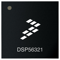
DSP56321VF220 Freescale Semiconductor, DSP56321VF220 Datasheet - Page 64

DSP56321VF220
Manufacturer Part Number
DSP56321VF220
Description
IC DSP 24BIT 220MHZ 196-BGA
Manufacturer
Freescale Semiconductor
Series
DSP563xxr
Type
Fixed Pointr
Datasheet
1.DSP56321VL200R2.pdf
(84 pages)
Specifications of DSP56321VF220
Interface
Host Interface, SSI, SCI
Clock Rate
220MHz
Non-volatile Memory
ROM (576 B)
On-chip Ram
576kB
Voltage - I/o
3.30V
Voltage - Core
1.60V
Operating Temperature
-40°C ~ 100°C
Mounting Type
*
Package / Case
196-MAPBGA
Device Core Size
24b
Format
Fixed Point
Clock Freq (max)
220MHz
Mips
220
Device Input Clock Speed
220MHz
Ram Size
576KB
Operating Supply Voltage (typ)
1.6/3.3V
Operating Supply Voltage (min)
1.5/3/3/3/3/3/3V
Operating Temp Range
-40C to 100C
Operating Temperature Classification
Industrial
Mounting
Surface Mount
Pin Count
196
Package Type
MA-BGA
Package
196MA-BGA
Numeric And Arithmetic Format
Fixed-Point
Maximum Speed
220 MHz
Device Million Instructions Per Second
220 MIPS
Lead Free Status / RoHS Status
Contains lead / RoHS non-compliant
Available stocks
Company
Part Number
Manufacturer
Quantity
Price
Company:
Part Number:
DSP56321VF220
Manufacturer:
XILINX
Quantity:
615
Company:
Part Number:
DSP56321VF220
Manufacturer:
Freescale Semiconductor
Quantity:
10 000
Design Considerations
The maximum internal current (I
case operation conditions—not necessarily a real application case. The typical internal current (I
reflects the average switching of the internal buses on typical operating conditions.
Perform the following steps for applications that require very low current consumption:
One way to evaluate power consumption is to use a current-per-MIPS measurement methodology to minimize
specific board effects (that is, to compensate for measured board current not caused by the DSP). A benchmark
power consumption test algorithm is listed in Appendix A. Use the test algorithm, specific test current
measurements, and the following equation to derive the current-per-MIPS value.
Where:
Note: F1 should be significantly less than F2. For example, F2 could be 66 MHz and F1 could be 33 MHz. The
4.4 Input (EXTAL) Jitter Requirements
The allowed jitter on the frequency of
(that is, it does not jump between the minimum and maximum values in one cycle) or the frequency of the jitter is
fast (that is, it does not stay at an extreme value for a long time), then the allowed jitter can be 2 percent. The phase
and frequency jitter performance results are valid only if the input jitter is less than the prescribed values.
4-4
1.
2.
3.
4.
5.
6.
7.
degree of difference between F1 and F2 determines the amount of precision with which the current rating
can be determined for an application.
Equation 4:
Equation 5:
Set the EBD bit when you are not accessing external memory.
Minimize external memory accesses, and use internal memory accesses.
Minimize the number of pins that are switching.
Minimize the capacitive load on the pins.
Connect the unused inputs to pull-up or pull-down resistors.
Disable unused peripherals.
Disable unused pin activity (for example,
I
I
F2
F1
⁄
typF2
typF1
I
MIPS
=
50
×
=
=
=
=
CCI
=
10
I
–
max) value reflects the typical possible switching of the internal buses on best-
⁄
12
MHz
current at F2
current at F1
high frequency (any specified operating frequency)
low frequency (any specified operating frequency lower than F2)
EXTAL
×
DSP56321 Technical Data, Rev. 11
3.3
=
×
is 0.5 percent. If the rate of change of the frequency of
(
33
I
typF2
×
10
–
6
I
CLKOUT
typF1
=
5.48 mA
)
⁄
(
,
F2 F1
XTAL
–
).
)
Freescale Semiconductor
CCItyp
EXTAL
) value
is slow


