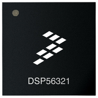
DSP56321VF200 Freescale Semiconductor, DSP56321VF200 Datasheet - Page 56

DSP56321VF200
Manufacturer Part Number
DSP56321VF200
Description
IC DSP 24BIT 200MHZ 196-BGA
Manufacturer
Freescale Semiconductor
Series
DSP563xxr
Type
Fixed Pointr
Datasheet
1.DSP56321VL200R2.pdf
(84 pages)
Specifications of DSP56321VF200
Interface
Host Interface, SSI, SCI
Clock Rate
200MHz
Non-volatile Memory
ROM (576 B)
On-chip Ram
576kB
Voltage - I/o
3.30V
Voltage - Core
1.60V
Operating Temperature
-40°C ~ 100°C
Mounting Type
*
Package / Case
196-MAPBGA
Lead Free Status / RoHS Status
Contains lead / RoHS non-compliant
Available stocks
Company
Part Number
Manufacturer
Quantity
Price
Company:
Part Number:
DSP56321VF200
Manufacturer:
MOT
Quantity:
1 831
Company:
Part Number:
DSP56321VF200
Manufacturer:
Freescale Semiconductor
Quantity:
10 000
Company:
Part Number:
DSP56321VF200R2
Manufacturer:
Freescale Semiconductor
Quantity:
10 000
Packaging
3-6
Note:
Ball
M10
M11
M12
No.
L11
L12
L13
L14
M1
M2
M3
M4
M5
M6
M7
M8
M9
Signal names are based on configured functionality. Most connections supply a single signal. Some connections provide a signal
with dual functionality, such as the MODx/IRQx pins that select an operating mode after RESET is deasserted but act as interrupt
lines during operation. Some signals have configurable polarity; these names are shown with and without overbars, such as
HAS/HAS. Some connections have two or more configurable functions; names assigned to these connections indicate the function
for a specific configuration. For example, connection N2 is data line H7 in non-multiplexed bus mode, data/address line HAD7 in
multiplexed bus mode, or GPIO line PB7 when the GPIO function is enabled for this pin. Unlike the TQFP package, most of the
GND pins are connected internally in the center of the connection array and act as heat sink for the chip.
GND
V
A3
A4
HA1, HA8, or PB9
HA2, HA9, or PB10
HA0, HAS/HAS, or PB8
V
H0, HAD0, or PB0
V
V
EXTAL
Reserved
NC
WR
RD
CCA
CCH
CCQL
CCQH
Signal Name
Table 3-1.
Ball
No.
M13
M14
N10
N11
N12
N13
N14
DSP56321 Technical Data, Rev. 11
N1
N2
N3
N4
N5
N6
N7
N8
N9
Signal List by Ball Number (Continued)
A1
A2
H6, HAD6, or PB6
H7, HAD7, or PB7
H4, HAD4, or PB4
H2, HAD2, or PB2
RESET
GND
AA3
NC
V
Reserved
BR
V
AA0
A0
CCQL
CCC
Signal Name
Ball
No.
P10
P11
P12
P13
P14
P1
P2
P3
P4
P5
P6
P7
P8
P9
NC
H5, HAD5, or PB5
H3, HAD3, or PB3
H1, HAD1, or PB1
NC
GND
AA2
XTAL
V
TA
BB
AA1
BG
NC
CCC
Freescale Semiconductor
Signal Name


