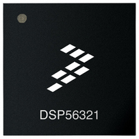
DSP56321VL200 Freescale Semiconductor, DSP56321VL200 Datasheet - Page 26

DSP56321VL200
Manufacturer Part Number
DSP56321VL200
Description
IC DSP 24BIT 200MHZ 196-MAPBGA
Manufacturer
Freescale Semiconductor
Series
DSP563xxr
Type
Fixed Pointr
Datasheet
1.DSP56321VL200R2.pdf
(84 pages)
Specifications of DSP56321VL200
Interface
Host Interface, SSI, SCI
Clock Rate
200MHz
Non-volatile Memory
ROM (576 B)
On-chip Ram
576kB
Voltage - I/o
3.30V
Voltage - Core
1.60V
Operating Temperature
-40°C ~ 100°C
Mounting Type
*
Package / Case
196-MAPBGA
Lead Free Status / RoHS Status
Lead free / RoHS Compliant
Available stocks
Company
Part Number
Manufacturer
Quantity
Price
Company:
Part Number:
DSP56321VL200
Manufacturer:
Freescale Semiconductor
Quantity:
10 000
Company:
Part Number:
DSP56321VL200R2
Manufacturer:
Freescale Semiconductor
Quantity:
10 000
Specifications
2.4.4
2-6
Notes:
No.
10 Delay from asynchronous RESET
13 Mode select setup time
14 Mode select hold time
15 Minimum edge-triggered interrupt
16 Minimum edge-triggered interrupt
17 Delay from IRQA, IRQB, IRQC, IRQD,
18 Delay from IRQA, IRQB, IRQC, IRQD,
19 Delay from address output valid
8
9
Delay from RESET assertion to all
pins at reset value
Required RESET duration
•
•
•
•
•
•
deassertion to first external address
output (internal reset deassertion)
•
•
request assertion width
request deassertion width
NMI assertion to external memory
access address out valid
•
•
NMI assertion to general-purpose
transfer output valid caused by first
interrupt instruction execution
caused by first interrupt instruction
execute to interrupt request
deassertion for level sensitive fast
interrupts
Power on, external clock
generator, DPLL disabled
Power on, external clock
generator, DPLL enabled
Power on, internal oscillator
During STOP, XTAL disabled
During STOP, XTAL enabled
During normal operation
Minimum
Maximum
Caused by first interrupt instruction
fetch
Caused by first interrupt instruction
execution
1.
2.
3.
4.
5.
6.
Characteristics
Reset, Stop, Mode Select, and Interrupt Timing
1, 6, 7
Characteristics
Refer to the DSP56321 User’s Manual for a detailed description of register reset values.
The total multiplication factor (MF) includes both integer and fractional parts (that is, MF = MFI + MFN/MFD).
The numerator (MFN) should be less than the denominator (MFD).
DPLL lock procedure duration is specified for the case when an external clock source is supplied to the EXTAL pin.
Frequency-only Lock Mode or non-integer MF, after partial reset.
Frequency and Phase Lock Mode, integer MF, after full reset.
3
4
Table 2-6.
Table 2-7.
Symbol
(WS + 3.75) × T
3.25 × T
4.25 × T
7.25 × T
CLKGEN and DPLL Characteristics (Continued)
Reset, Stop, Mode Select, and Interrupt Timing
Expression
75000 × ET
75000 × ET
DSP56321 Technical Data, Rev. 11
1000 × ET
50 × ET
2.5 × T
2.5 × T
8.9 × T
10.94
Min
—
200 MHz
C
C
C
+ 2.0
+ 2.0
+ 2.0
C
C
C
C
C
C
C
C
Max
–
250.0
0.375
0.375
18.25
23.25
38.25
Min
12.5
30.0
44.5
5.0
0.0
4.0
4.0
17
—
—
—
200 MHz
Min
220 MHz
Note 7
Max
180
26
—
—
—
—
—
—
—
—
—
—
—
—
—
—
Max
227.5
0.341
0.341
11.38
16.77
21.24
34.99
40.45
Min
4.55
30.0
0.0
4.0
4.0
16
—
—
—
220 MHz
Min
Note 7
Max
163
240 MHz
26
—
—
—
—
—
—
—
—
—
—
—
—
—
—
208.5
0.313
0.313
10.43
15.55
19.72
32.23
Max
Min
4.17
30.0
37.0
0.0
4.0
4.0
15
240 MHz
—
—
—
5
Note 7
Max
150
Freescale Semiconductor
26
—
—
—
—
—
—
—
—
—
—
—
—
—
—
Min
275 MHz
182.0
0.273
0.273
13.82
17.45
28.36
32.37
Min
3.64
30.0
9.1
9.1
0.0
4.0
4.0
—
—
—
275 MHz
Max
Note 7
Max
140
26
—
—
—
—
—
—
—
—
—
—
—
—
—
—
Unit
Unit
ms
ms
ns
ns
µs
ns
ns
ns
ns
ns
ns
ns
ns
ns
ns
ns
ns


