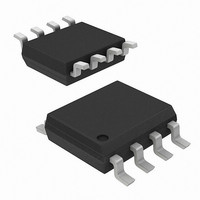
ALD114904SAL Advanced Linear Devices Inc, ALD114904SAL Datasheet - Page 2

ALD114904SAL
Manufacturer Part Number
ALD114904SAL
Description
MOSFET N-CH 10.6V DUAL 8SOIC
Manufacturer
Advanced Linear Devices Inc
Series
EPAD®r
Datasheet
1.ALD114904PAL.pdf
(11 pages)
Specifications of ALD114904SAL
Package / Case
8-SOIC (0.154", 3.90mm Width)
Fet Type
2 N-Channel (Dual)
Fet Feature
Depletion Mode
Drain To Source Voltage (vdss)
10.6V
Vgs(th) (max) @ Id
360mV @ 1µA
Power - Max
500mW
Mounting Type
Surface Mount
Minimum Operating Temperature
0 C
Configuration
Dual
Transistor Polarity
N-Channel
Resistance Drain-source Rds (on)
500 Ohms
Forward Transconductance Gfs (max / Min)
0.0014 S
Drain-source Breakdown Voltage
10 V
Gate-source Breakdown Voltage
10.6 V
Continuous Drain Current
12 mA
Power Dissipation
500 mW
Maximum Operating Temperature
+ 70 C
Mounting Style
SMD/SMT
Lead Free Status / RoHS Status
Lead free / RoHS Compliant
Gate Charge (qg) @ Vgs
-
Current - Continuous Drain (id) @ 25° C
-
Rds On (max) @ Id, Vgs
-
Lead Free Status / Rohs Status
Lead free / RoHS Compliant
Other names
1014-1064
ABSOLUTE MAXIMUM RATINGS
Drain-Source voltage,
Gate-Source voltage,
Power dissipation
Operating temperature range SCL, PCL, SAL, PAL package
Storage temperature range
Lead temperature, 10 seconds
OPERATING ELECTRICAL CHARACTERISTICS
V + = +5V V- = GND T A = 25
CAUTION: ESD Sensitive Device. Use static control procedures in ESD controlled environment.
Notes:
ALD114804/ALD114804A/ALD114904/ALD114904A
Gate Threshold Voltage
Offset Voltage
V GS1 -V GS2
V GS1 -V GS2 Tempco
GateThreshold Tempco
On Drain Current
Forward Transconductance
Transconductance Mismatch
Output Conductance
Drain Source On Resistance
Drain Source On Resistance
Drain Source On Resistance
Tolerance
Drain Source On Resistance
Mismatch
Drain Source Breakdown
Voltage
Drain Source Leakage Current
Gate Leakage Current
Transfer Reverse Capacitance
Turn-on Delay Time
Turn-off Delay Time
Crosstalk
Input Capacitance
Parameter
1
Consists of junction leakage currents
1
V
V
GS
DS
1
V GS(th)
V OS
∆V OS
∆V GS(th)
I DS (ON)
G FS
∆G FS
G OS
R DS (ON)
R DS (ON)
∆R DS (ON)
∆R DS (ON)
BV DSX
I DS (OFF)
I GSS
C ISS
C RSS
t on
t off
Symbol
°
C unless otherwise specified
ALD114804A / ALD114904A ALD114804 / ALD114904
Min
-0.42
10
Typ
-0.40
+1.6
12.0
-1.7
500
0.0
3.0
1.4
1.8
5.4
0.5
2.5
0.1
Advanced Linear Devices
68
10
10
10
10
60
2
5
3
-0.38
Max
400
200
5
4
1
-0.44
Min
10
-0.40
+1.6
12.0
Typ
-1.7
500
0.0
3.0
1.4
1.8
5.4
0.5
2.5
0.1
68
10
10
10
10
60
7
5
3
-0.36
Max
400
200
20
4
1
-65°C to +150°C
Unit
V
mV
µV/ °C
mV/ °C
%
Ω
KΩ
%
%
V
nA
nA
ns
ns
mA
mmho
µmho
pA
pF
pF
dB
pA
0°C to +70°C
500 mW
+260°C
Test Condition
I DS =1µA, V DS = 0.1V
I DS =1µA
V DS1 = V DS2
I D = 1µA, V DS = 0.1V
I D = 20µA, V DS = 0.1V
I D = 40µA, V DS = 0.1V
V GS = +9.1V, V DS = +5V
V GS = +3.6V, V DS = +5V
V GS =+3.6 V
V DS = +8.6V
VGS =+3.6V
V DS = +8.6V
V DS = 0.1V
VGS = +3.6V
V DS = 0.1V
V GS = +0.0V
I DS = 1.0µA
V GS = -1.4V
V GS = -1.4V, V DS =+5V
T A = 125°C
V DS = 0V, V GS = +5V
T A =125°C
V + = 5V R L = 5KΩ
V + = 5V R L = 5KΩ
f = 100KHz
10.6V
10.6V
2 of 11


