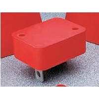
90065-019 Littelfuse Inc, 90065-019 Datasheet - Page 8

90065-019
Manufacturer Part Number
90065-019
Description
VARISTOR 820V 550J 40MM MIL DB
Manufacturer
Littelfuse Inc
Series
DBr
Specifications of 90065-019
Energy
550J
Varistor Voltage
820V
Current-surge
28.8kA
Number Of Circuits
1
Maximum Ac Volts
510VAC
Package / Case
Chassis Mount
Capacitance Value
2500pF
Clamping Current
200A
Clamping Voltage
1350V
Lead Style
Solder Lug
Ac Voltage Rating (max)
510VAC
Mounting
Bolt-Down
Surge Current (max)
28800A
Product
MOV
Voltage Rating Dc
820 V
Voltage Rating Ac
510 V
Peak Surge Current
200 A
Capacitance
2500 pF
Operating Temperature Range
- 55 C to + 125 C
Dimensions
40 mm Dia.
Termination Style
Axial
Lead Free Status / RoHS Status
Contains lead / RoHS non-compliant
Maximum Dc Volts
-
Lead Free Status / Rohs Status
Lead free / RoHS Compliant
Varistor Products
High Reliability Varistors
Aerospace and Military
Neutron Effects
A second MOV-zener comparison was made in response to neutron
fluence. The selected devices were equal in area.
Figure 2 shows the clamping voltage response of the MOV and the zener
to neutron irradiation to as high as 10
trast to the large change in the zener, the MOV is unaltered. At higher-
currents where the MOV’s clamping voltage is again unchanged, the
zener device clamping voltage increases by as much as 36%.
Counterclockwise rotation of the V-I characteristics is observed in silicon
devices at high neutron irradiation levels; in other words, increasing
leakage at low current levels and increasing clamping voltage at higher
current levels.
The solid and open circles for a given fluence represent the high and low
breakdown currents for the sample of devices tested. Note that there is a
marked decrease in current (or energy) handling capability with
increased neutron fluence.
Failure threshold of silicon semiconductor junctions is further reduced
when high or rapidly increasing currents are applied. Junctions develop
hot spots, which enlarge until a short occurs if current is not limited or
quickly removed.
The characteristic voltage current relationship of a PN-Junction is shown
in Figure 3.
152
300
200
100
80
60
50
40
30
20
10
FIGURE 2. V-I CHARACTERISTIC RESPONSE TO NEUTRON
10
VARISTOR V130A2
INITIAL A T 10
10
IRRADIA TION FOR MOV AND ZENER DIODE
DEVICES
10
15
8
10
AMPERES
1.5K 200 INITIAL
7
15
N/cm
10
6
1.5K 200
AT 10
2
. It is apparent that in con-
15
10
5
10
4
w w w . l i t t e l f u s e . c o m
10
3
At low reverse voltage, the device will conduct very little current (the
saturation current). At higher reverse voltage V BO (breakdown
voltage),the current increases rapidly as the electrons are either pulled
by the electric field (Zener effect) or knocked out by other electrons
(avalanching). A further increase in voltage causes the device to exhibit
a negative resistance characteristic leading to secondary breakdown.
This manifests itself through the formation of hotspots, and irreversible
damage occurs. This failure threshold decreases under neutron irradia-
tion for zeners, but not for Zinc Oxide Varistors.
Gamma Radiation
Radiation damage studies were performed on type V130LA2 varistors.
Emission spectra and V-I characteristics were collected before and after
irradiation with 10
Both show no change, within experimental error, after irradiation.
REDUCTION IN
FAILURE STRESSHOLD
BY RADIAL
FIGURE 3. V-I CHARACTERISTIC OF PN-JUNCTION
BREAKDO WN
VOLTAGE
6
rads Co
BREAKDO WN
SECONDARY
60
gamma radiation.
SATURATION
CURRENT
REVERSE
BIAS
I
FORWARD
BIAS
V


