CS8371ETVA7 ON Semiconductor, CS8371ETVA7 Datasheet

IC REG LIN DUAL 8/5V VRT TO220-7

CS8371ETVA7

Manufacturer Part Number
CS8371ETVA7
Description
IC REG LIN DUAL 8/5V VRT TO220-7
Manufacturer
ON Semiconductor
Datasheet

Specifications of CS8371ETVA7

Regulator Topology
Positive Fixed
Voltage - Output
8V, 5V
Voltage - Input
7 ~ 26 V
Number Of Regulators
2
Current - Output
1A, 250mA
Current - Limit (min)
1.1A, 270mA
Operating Temperature
-40°C ~ 85°C
Mounting Type
Through Hole
Package / Case
TO-220-7 (Bent and Staggered Leads)
Polarity
Positive
Number Of Outputs
2
Output Type
Fixed
Output Voltage
5 V, 8 V
Output Current
1 A, 0.25 A
Line Regulation
50 mV
Load Regulation
150 mV
Dropout Voltage (max)
1.2 V
Input Voltage Max
12.5 V
Maximum Operating Temperature
+ 85 C
Minimum Operating Temperature
- 40 C
Mounting Style
Through Hole
Voltage Regulation Accuracy
5 %
Lead Free Status / RoHS Status
Contains lead / RoHS non-compliant
Voltage - Dropout (typical)
-
Lead Free Status / Rohs Status
Lead free / RoHS Compliant
Other names
CS8371ETVA7OS
CS8371
8.0 V/1.0 A, 5.0 V/250 mA
Dual Regulator
with Independent Output
Enables and NOCAPt
8.0 V ±5.0% output sources 1.0 A, while the 5.0 V ±5.0% output
sources 250 mA. Each output is controlled by its own ENABLE lead.
Setting the ENABLE input high turns on the associated regulator
output. Holding both ENABLE inputs low puts the IC into sleep mode
where current consumption is less than 10 mA.
thermal runaway conditions. The device can withstand 45 V load dump
transients making suitable for use in automotive environments. ON’s
proprietary NOCAP solution is the first technology which allows the
output to be stable without the use of an external capacitor.
tab. The tab can be connected to a heatsink if necessary.
Features
*For additional information on our Pb−Free strategy and soldering details, please
© Semiconductor Components Industries, LLC, 2006
June, 2006 − Rev. 12
download the ON Semiconductor Soldering and Mounting Techniques
Reference Manual, SOLDERRM/D.
The CS8371 is an 8.0 V/5.0 V dual output linear regulator. The
The regulator is protected against overvoltage, short−circuit and
The CS8371 is available in a 7 lead TO−220 package with copper
Two Regulated Outputs
Independent ENABLE for Each Output
Seperate Sense Feedback Lead for 8.0 V Output
< 10 mA Sleep Mode Current
Fault Protection
CMOS Compatible, Low Current ENABLE Inputs
Pb−Free Packages are Available*
8.0 V ±5.0%; 1.0 A
5.0 V ±5.0%; 250 mA
Overvoltage Shutdown
+45 V Peak Transient Voltage
Short Circuit
Thermal Shutdown
1
CS8371ET7
CS8371ET7G
CS8371ETVA7
CS8371ETVA7G
AWLYWWG
1
1
Device
7
8371
ORDERING INFORMATION
CS
PIN CONNECTIONS AND
A
WL
Y
WW
G
MARKING DIAGRAM
http://onsemi.com
= Assembly Location
= Wafer Lot
= Year
= Work Week
= Pb−Free Package
AWLYWWG
STRAIGHT
STRAIGHT
VERTICAL
VERTICAL
(Pb−Free)
(Pb−Free)
Package
TO−220
TO−220
TO−220
TO−220
Publication Order Number:
8371
CS
SEVEN LEAD
SEVEN LEAD
TVA SUFFIX
CASE 821E
CASE 821J
T SUFFIX
TO−220
TO−220
Tab = GND
Pin 1. ENABLE
50 Units/Rail
50 Units/Rail
50 Units/Rail
50 Units/Rail
Shipping
2. ENABLE
3. V
4. GND
5. Sense
6. V
7. V
CS8371/D
OUT2
CC
OUT1
1
2

Related parts for CS8371ETVA7

CS8371ETVA7 Summary of contents

Page 1

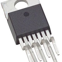
... Work Week G = Pb−Free Package ORDERING INFORMATION Device Package CS8371ET7 TO−220 STRAIGHT CS8371ET7G TO−220 STRAIGHT (Pb−Free) CS8371ETVA7 TO−220 VERTICAL CS8371ETVA7G TO−220 VERTICAL (Pb−Free) 1 TO−220 SEVEN LEAD T SUFFIX CASE 821E TO−220 SEVEN LEAD TVA SUFFIX CASE 821J Tab = GND Pin 1. ENABLE 1 2 ...

Page 2

V CC ENABLE − 1.2 V ENABLE − 1.2 V GND MAXIMUM RATINGS Power Dissipation ENABLE Input Voltage Range Load Current (8.0 V Regulator) Load Current (5.0 V Regulator) Transient Peak Voltage (31 V Load Dump ...

Page 3

ELECTRICAL CHARACTERISTICS 5.0 mA, unless otherwise stated.) OUT1 OUT2 Characteristic PRIMARY OUTPUT (V ) OUT1 Output Voltage I OUT1 10.5 V ≤ V Line Regulation 5.0 mA ≤ I Load Regulation Sleep Mode Quiescent Current V ...

Page 4

PACKAGE PIN DESCRIPTION PACKAGE LEAD # 7 Lead TO−220 TYPICAL PERFORMANCE CHARACTERISTICS 8. 8. 1.0 A OUT 8.03 8.02 8.01 8.00 7.99 7.98 7.97 7.96 7.95 ...

Page 5

TYPICAL PERFORMANCE CHARACTERISTICS 25° Reg 1 Output Current (A) Figure 6. Regulator 1 Current Limit 9.0 Enable 1 ...

Page 6

TYPICAL PERFORMANCE CHARACTERISTICS 8.020 8.015 8.010 8.005 −40°C 8.000 25°C 7.995 7.990 7.985 7.980 0 100 200 300 400 500 600 700 800 900 1000 Output Current (mA) Figure 12. Regulator 1 Load Regulation = ...

Page 7

TYPICAL PERFORMANCE CHARACTERISTICS OUT 25° −1 −2 −3 1000 Time (ms) Figure 18. Regulator 1 Load Transient Response 100 ...

Page 8

... ESR (Equivalent Series Resistance) and board layout parasitics all can create oscillations if not properly accounted for. NOCAP Semiconductor exclusive output stage which internally compensates the LDO regulator over temperature, load and line variations without the need for an expensive external capacitor. It incorporates high gain (> ...

Page 9

This will depend on the load conditions. With these types of loads, a traditional output stage may be better suited for proper operation. Output 1 employs NOCAP. Refer to the plots in the ...

Page 10

OPTIONAL CHAMFER SEATING PLANE −Q− 0.356 (0.014 CS8371 PACKAGE DIMENSIONS 7 LEAD, TO−220 T SUFFIX CASE 821E−04 ISSUE ...

Page 11

... Opportunity/Affirmative Action Employer. This literature is subject to all applicable copyright laws and is not for resale in any manner. PUBLICATION ORDERING INFORMATION LITERATURE FULFILLMENT: Literature Distribution Center for ON Semiconductor P.O. Box 5163, Denver, Colorado 80217 USA Phone: 303−675−2175 or 800−344−3860 Toll Free USA/Canada Fax: 303− ...

Related keywords