CS8321YDPR3 ON Semiconductor, CS8321YDPR3 Datasheet - Page 3
CS8321YDPR3
Manufacturer Part Number
CS8321YDPR3
Description
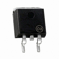
IC REG LDO LIN 150MA 5V D2PAK-3
Manufacturer
ON Semiconductor
Datasheet
1.CS8321YDPR3.pdf
(6 pages)
Specifications of CS8321YDPR3
Regulator Topology
Positive Fixed
Voltage - Output
5V
Voltage - Input
6 ~ 26 V
Voltage - Dropout (typical)
0.3V @ 150mA
Number Of Regulators
1
Current - Output
150mA
Current - Limit (min)
175mA
Operating Temperature
-40°C ~ 125°C
Mounting Type
Surface Mount
Package / Case
TO-263-3, D²Pak (3 leads + Tab), TO-263AA
Lead Free Status / RoHS Status
Contains lead / RoHS non-compliant
Other names
CS8321YDPR3OS


of an error amplifier, bandgap voltage reference, PNP pass
transistor with antisaturation control, and current limit.
Q
As Q
begins to rise as Q
capacitor. Once V
amplifier becomes biased and provides the appropriate
amount of base current to Q
the scaled output voltage via an internal voltage divider, R1
and R2, and compares it to the bandgap voltage reference.
The error amplifier’s output is a current which is equal to the
error amplifier’s differential input voltage times its
transconductance. Therefore, the error amplifier varies the
base drive current to Q
on the difference between the reference voltage and the
scaled output voltage, V
Antisaturation Protection
prevent the pass transistor from going into deep saturation,
which would cause excessive power dissipation due to large
bias currents lost to the substrate via a parasitic PNP
transistor, as shown in Figure 2.
Current Limit Limit
conditions. As shown in Figure 3, the output current will fold
back when the faulted load is continually increased. This
technique has been incorporated to limit the total power
dissipation across the device during a short circuit condition,
since the device does not contain overtemperature
shutdown.
three main characteristics of a linear regulator: startïup
delay, load transient response and loop stability.
N
The CS8321 is a series pass voltage regulator. It consists
As the voltage at the input, V
An antisaturation control circuit has also been added to
The output stage is protected against short circuit
The output or compensation capacitor helps determine
VOLTAGE REFERENCE AND OUTPUT CIRCUITRY
Figure 2. The Parasitic PNP Transistor Which Is
is forward biased via R. Q
P
becomes forward biased, the output voltage, V
Part of the Pass Transistor (Q
Q
Parasitic
STABILITY CONSIDERATIONS
Substrate
OUT
P
’s output current charges the output
N
rises to a certain level, the error
, which provides bias to Q
OUT
P
.
. The error amplifier monitors
N
CIRCUIT DESCRIPTION AND APPLICATION NOTES
IN
provides base drive for Q
, is increased (Figure 1),
Q
P
V
P
) Structure
V
OUT
IN
P
, based
http://onsemi.com
OUT
P
CS8321
.
,
3
availability, size and temperature constraints. A tantalum or
aluminum electrolytic capacitor is best, since a film or
ceramic capacitor with almost zero ESR can cause
instability. The aluminum electrolytic capacitor is the least
expensive solution, but, if the circuit operates at low
temperatures (ï25°C to ï40°C), both the value and ESR of
the capacitor will vary considerably. The capacitor
manufacturers data sheet usually provides this information.
4 should work for most applications, however it is not
necessarily the best solution.
application, start with a tantalum capacitor of the
V
The capacitor value and type should be based on cost,
The value for the output capacitor C
To determine an acceptable value for C
IN
0.34257
0.30831
0.27405
0.23980
0.20554
0.17128
0.13703
0.10277
0.06851
0.03426
Figure 4. Test and Application Circuit Showing
**C
Figure 3. Typical Current Limit and Fold Back
0.1 mF
*C
†Pin internally shorted to V
supply filter.
minimum temperature expected.
0.0
C
IN
OUT
0.0
IN
required if regulator is located far from the power
*
required for stability. Capacitor must operate at
0.51 1.02 1.52 2.03 2.54 3.05 3.56 4.06 4.57 5.08
Output Compensation
Waveform
CS8321
Curve will vary with temperature
and process variation.
V
OUT
Output Voltage
OUT
Sense†
V
in 3ïpin applications.
OUT
OUT
OUT
shown in Figure
for a particular
C
0.1 mF
OUT
**
Related parts for CS8321YDPR3
Image
Part Number
Description
Manufacturer
Datasheet
Request
R

Part Number:
Description:
ON Semiconductor [VOLTAGE REGULATOR]
Manufacturer:
ON Semiconductor
Datasheet:
Part Number:
Description:
357-036-542-201 CARDEDGE 36POS DL .156 BLK LOPRO
Manufacturer:
ON Semiconductor
Datasheet:
Part Number:
Description:
357-036-542-201 CARDEDGE 36POS DL .156 BLK LOPRO
Manufacturer:
ON Semiconductor
Datasheet:
Part Number:
Description:
357-036-542-201 CARDEDGE 36POS DL .156 BLK LOPRO
Manufacturer:
ON Semiconductor
Datasheet:
Part Number:
Description:
357-036-542-201 CARDEDGE 36POS DL .156 BLK LOPRO
Manufacturer:
ON Semiconductor
Datasheet:
Part Number:
Description:
357-036-542-201 CARDEDGE 36POS DL .156 BLK LOPRO
Manufacturer:
ON Semiconductor
Datasheet:
Part Number:
Description:
357-036-542-201 CARDEDGE 36POS DL .156 BLK LOPRO
Manufacturer:
ON Semiconductor
Datasheet:
Part Number:
Description:
357-036-542-201 CARDEDGE 36POS DL .156 BLK LOPRO
Manufacturer:
ON Semiconductor
Datasheet:
Part Number:
Description:
357-036-542-201 CARDEDGE 36POS DL .156 BLK LOPRO
Manufacturer:
ON Semiconductor
Datasheet:
Part Number:
Description:
357-036-542-201 CARDEDGE 36POS DL .156 BLK LOPRO
Manufacturer:
ON Semiconductor
Datasheet:
Part Number:
Description:
357-036-542-201 CARDEDGE 36POS DL .156 BLK LOPRO
Manufacturer:
ON Semiconductor
Datasheet:
Part Number:
Description:
Manufacturer:
ON Semiconductor
Datasheet:
Part Number:
Description:
Manufacturer:
ON Semiconductor
Datasheet:
Part Number:
Description:
Manufacturer:
ON Semiconductor
Datasheet: