SP721APP Littelfuse Inc, SP721APP Datasheet - Page 2
SP721APP
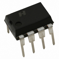
Manufacturer Part Number
SP721APP
Description
TVS ARRAY ESD 6 INPUT 8-DIP
Manufacturer
Littelfuse Inc
Series
SP721r
Type
Dioder
Specifications of SP721APP
Package / Case
8-DIP
Voltage - Working
30V
Technology
Mixed Technology
Number Of Circuits
6
Applications
General Purpose
Current Rating
+/- 5 A
Forward Voltage Drop
2 V
Operating Voltage
2 V to 30 V
Channels
6 Channels
Capacitance
3 pF
Operating Temperature Range
- 40 C to + 105 C
Brand/series
SP721 Series
Current, Surge
±3 A
Dimensions
10.16mmL×7.11mmW×4.95mmH
Mounting Type
SMD
Primary Type
Transient Voltage Surge Suppressor
Voltage, Supply
2 to 30 V
Lead Free Status / RoHS Status
Lead free / RoHS Compliant
Power (watts)
-
Voltage - Clamping
-
Lead Free Status / Rohs Status
Lead free / RoHS Compliant
Other names
F2720
Available stocks
Company
Part Number
Manufacturer
Quantity
Price

Part Number:
SP721APP
Manufacturer:
LITTELFUSE/力特
Quantity:
20 000


CAUTION: Stresses above those listed in “Absolute Maximum Ratings” may cause
permanent damage to the device. This is a stress only rating and operation of the device
at these or any other conditions above those indicated in the operational sections of this
specification is not implied.
Note:
ESD Ratings and Capability (Figure 1, Table 1)
Load Dump and Reverse Battery (Note 2)
Notes:
2. In automotive and battery operated systems, the power supply lines should be externally protected for load dump and reverse battery. When the V+ and V- Pins are connected to het same
3. Refer to the Figure 3 graph for definitions of equivalent “SCR ON Threshold” and “SCR ON Resistance” . These characteristics are given here for thumb-rule nformation to determine peak
(Application as an Input Clamp for Over-voltage, Greater
than 1V
SP721 Lead-Free/Green Series
Operating Voltage Range,
V
Forward Voltage Drop
Input Leakage Current
Quiescent Supply Current
Equivalent SCR ON Threshold
Equivalent SCR ON Resistance
Input Capacitance
Input Switching Speed
Absolute Maximum Ratings
Electrical Characteristics
Typical Application of the SP721
supply voltage source as the device or control line under protection, a current limiti ng resistor should be connected in series between the external supply and the SP721 supply pins to
limit reverse battery current to within the rated maximum limits. Bypass capacitors of typically 0.01μF or larger romf the V+ and V- Pins to ground are recommended.
current and dissipation under EOS conditions.
Continuous Supply Voltage, (V+) - (V-)
Forward Peak Current, I
(Refer to Figure 5)
SUPPLY
IN to V-
IN to V+
BE
SOURCES
= [(V+) - (V-)]
DRIVERS
SIGNAL
INPUT
OR
Above V+ or less than -1V
+V
SP721 INPUT PROTECTION CIRCUIT (1 OF 6 SHO WN)
SP721
CC
Parameter
Parameter
IN 1 - 3
IN
to V
CC
T
A
, I
= -40
IN
BE
IN
to GND
- 7
below V-)
o
C to 105
Symbol
I
QUIESCENT
V
V
V
TVS Diode Arrays
General Purpose ESD Protection - SP721 Series
SUPPLY
C
FWDH
t
FWDL
I
ON
IN
IN
±2A, 100μs
LINEAR OR
DIGITAL IC
INTERFACE
o
C, V
V+
Rating
V-
TO +V
+35
+V
IN
CC
CC
= 0.5V
I
IN
Test Conditions
V
= 1A (Peak Pulse)
FWD
CC
/I
Units
Note 3
FWD
, Unless Otherwise Specified
Revision: April 14, 2011
V
V
; Note 3
62
1.
Thermal Information
Maximum Junction Temperature (Plastic
Package)
Maximum Lead Temperature (Soldering 10s)
(SOIC Lead Tips Only)
JA
Thermal Resistance (Typical, Note 1)
Maximum Storage Temperature Range
(SPA
is measured with the component mounted on an evaluation PC board in free air.
PDIP Package
SOIC Package
™
Min
-20
-
-
-
-
-
-
-
-
Family of Products)
Parameter
2 to 30
Please refer to
Typ
1.1
50
2
2
5
1
3
2
Specifications are subject to change without notice.
www.littelfuse.com/SPA
Max
+20
200
-
-
-
-
-
-
-
-65 to 150
Rating
160
170
150
260
for current information.
JA
©2011 Littelfuse, Inc.
Units
nA
nA
W
pF
ns
V
V
V
V
Units
o
o
o
C/W
C/W
C/W
o
o
o
C
C
C
Related parts for SP721APP
Image
Part Number
Description
Manufacturer
Datasheet
Request
R

Part Number:
Description:
IC,Overvoltage Protector,BIPOLAR,SOP,8PIN,PLASTIC
Manufacturer:
Littelfuse Inc
Datasheet:

Part Number:
Description:
FUSEHOLDER 20A MINI INLINE CRIMP
Manufacturer:
Littelfuse Inc
Datasheet:

Part Number:
Description:
FUSEHOLDER BODY ATO INLINE PNLMT
Manufacturer:
Littelfuse Inc
Datasheet:

Part Number:
Description:
FUSE 2A 63V FAST 1206
Manufacturer:
Littelfuse Inc
Datasheet:
Part Number:
Description:
FUSE 1.25A 63V FAST 1206
Manufacturer:
Littelfuse Inc
Datasheet:
Part Number:
Description:
FUSE .250A 125V FAST 1206
Manufacturer:
Littelfuse Inc
Datasheet:
Part Number:
Description:
FUSE 4A 32V FAST 1206
Manufacturer:
Littelfuse Inc
Datasheet:
Part Number:
Description:
FUSE 1.75A 63V FAST 1206
Manufacturer:
Littelfuse Inc
Datasheet:

Part Number:
Description:
FUSE 1A 32V FST 0603 LEADFREE TR
Manufacturer:
Littelfuse Inc
Datasheet:

Part Number:
Description:
FUSE 1A 32V FAST SLIM 0402
Manufacturer:
Littelfuse Inc
Datasheet:

Part Number:
Description:
FUSE 2A 125V FAST NANO2 SMD
Manufacturer:
Littelfuse Inc
Datasheet:

Part Number:
Description:
FUSE .250A 125V FAST NANO2 SMD
Manufacturer:
Littelfuse Inc
Datasheet:

Part Number:
Description:
FUSE .500A 125V FAST NANO2 SMD
Manufacturer:
Littelfuse Inc
Datasheet:

Part Number:
Description:
FUSE 1.5A 125V FAST NANO2 SMD
Manufacturer:
Littelfuse Inc
Datasheet:

Part Number:
Description:
FUSE 4A 125V FAST NANO2 SMD
Manufacturer:
Littelfuse Inc
Datasheet: