MIC29150-3.3BU Micrel Inc, MIC29150-3.3BU Datasheet - Page 7
MIC29150-3.3BU
Manufacturer Part Number
MIC29150-3.3BU
Description
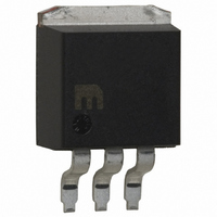
IC REG LDO 1.5A 3.3V TO263
Manufacturer
Micrel Inc
Datasheet
1.MIC29152WU_TR.pdf
(23 pages)
Specifications of MIC29150-3.3BU
Mounting Type
Surface Mount
Regulator Topology
Positive Fixed
Voltage - Output
3.3V
Voltage - Input
Up to 26V
Voltage - Dropout (typical)
0.35V @ 1.5A
Number Of Regulators
1
Current - Output
1.5A
Operating Temperature
-40°C ~ 125°C
Package / Case
TO-263-3, D²Pak (3 leads + Tab), TO-263AA
No. Of Pins
3
Peak Reflow Compatible (260 C)
No
Termination Type
SMD
Current Rating
1.5A
Output Voltage Max
3.3V
Leaded Process Compatible
No
Lead Free Status / RoHS Status
Lead free / RoHS Compliant
Current - Limit (min)
-
Lead Free Status / RoHS Status
Contains lead / RoHS non-compliant, Lead free / RoHS Compliant
Available stocks
Company
Part Number
Manufacturer
Quantity
Price

Part Number:
MIC29150-3.3BU
Manufacturer:
MICREL/麦瑞
Quantity:
20 000
Company:
Part Number:
MIC29150-3.3BUTR
Manufacturer:
FUJI
Quantity:
1 000


Notes:
1.
2.
3.
4.
5.
6.
7.
8.
9.
10. Thermal regulation is defined as the change in output voltage at a time T after a change in power dissipation is applied, excluding load or line
11. Comparator thresholds are expressed in terms of a voltage differential at the Adjust terminal below the nominal reference voltage measured at 6V
12. V
13. When used in dual supply systems where the regulator load is returned to a negative supply, the output voltage must be diode clamped to ground.
Micrel, Inc.
May 2010
Dropout voltage is defined as the input-to-output differential when the output voltage drops to 99% of its normal value with V
Devices are ESD sensitive. Handling precautions recommended.
Full load current (I
Maximum positive supply voltage of 60V must be of limited duration (<100msec) and duty cycle (≤1%). The maximum continuous supply voltage is
26V. Exceeding the absolute maximum rating may damage the device.
The device is not guaranteed to function outside its operating rating.
Specification for packaged product only.
V
current.
Ground pin current is the regulator quiescent current. The total current drawn from the source is the sum of the load current plus the ground pin
current.
Output voltage temperature coefficient is defined as the worst case voltage change divided by the total temperature range.
regulation effects. Specifications are for a200mA load pulse at VIN = 20V (a 4W pulse) for T = 10ms.
input. To express these thresholds in terms of output voltage change, multiply by the error amplifier gain = V
at a programmed output voltage of 5V, the Error output is guaranteed to go low when the output drops by 95mV x 5V/1.240V = 384mV. Thresholds
remain constant as a percent of V
IN
EN
= V
≤ 0.8V and V
OUT (nominal)
+ 1V. For example, use V
IN
FL
≤ 26V, V
) is defined as 1.5A for the MIC29150, 3A for the MIC29300, 5A for the MIC29500, and 7.5A for the MIC29750 families.
OUT
= 0.
OUT
as V
OUT
IN
= 4.3V for a 3.3V regulator or use 6V for a 5V regulator. Employ pulse-testing procedures to pin
is varied, with the dropout warning occurring at typically 5% below nominal, 7.7% guaranteed.
7
MIC29150/29300/29500/29750
OUT
/V
REF
= (R1 + R2)/R2. For example,
OUT
M9999-050510-B
+ 1V applied to V
IN
.
Related parts for MIC29150-3.3BU
Image
Part Number
Description
Manufacturer
Datasheet
Request
R

Part Number:
Description:
IC REG LDO 1.5A 12V TO-263-3
Manufacturer:
Micrel Inc
Datasheet:

Part Number:
Description:
IC REG LDO 1.5A 12V TO-220-3
Manufacturer:
Micrel Inc
Datasheet:

Part Number:
Description:
IC REG LDO 1.5A 3.3V TO263
Manufacturer:
Micrel Inc
Datasheet:
Part Number:
Description:
IC REG LDO 1.5A 5.0V TO263
Manufacturer:
Micrel Inc
Datasheet:
Part Number:
Description:
IC REG LDO 1.5A 3.3V TO220-3
Manufacturer:
Micrel Inc
Datasheet:
Part Number:
Description:
IC REG LDO 1.5A 5.0V TO220-3
Manufacturer:
Micrel Inc
Datasheet:
Part Number:
Description:
IC REG LDO 1.5A 5.0V TO263
Manufacturer:
Micrel Inc
Datasheet:

Part Number:
Description:
IC REG LDO 1.5A 12V TO-263
Manufacturer:
Micrel Inc
Datasheet:
Part Number:
Description:
IC REG LDO 1.5A 4.2V TO220-3
Manufacturer:
Micrel Inc
Datasheet:
Part Number:
Description:
IC,VOLT REGULATOR,FIXED,+12V,BIPOLAR,SIP,3PIN,PLASTIC
Manufacturer:
Micrel Inc
Datasheet:
Part Number:
Description:
IC REG LDO 1.5A 12V TO-263
Manufacturer:
Micrel Inc
Datasheet:
Part Number:
Description:
IC REG LDO 1.5A 3.3V TO-263
Manufacturer:
Micrel Inc
Datasheet:
Part Number:
Description:
IC REG LDO 1.5A 5.0V TO-263
Manufacturer:
Micrel Inc
Datasheet:
Part Number:
Description:
IC REG LDO 1.5A 12V TO-263
Manufacturer:
Micrel Inc
Datasheet:
Part Number:
Description:
IC REG LDO 1.5A 3.3V TO-263
Manufacturer:
Micrel Inc
Datasheet: