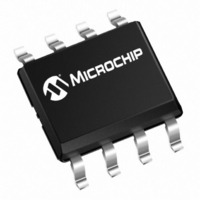
TC1300R-2.8VUA Microchip Technology, TC1300R-2.8VUA Datasheet - Page 3

TC1300R-2.8VUA
Manufacturer Part Number
TC1300R-2.8VUA
Description
IC REG LDO 2.8V 300MA SD 8MSOP
Manufacturer
Microchip Technology
Datasheet
1.TC1300R-2.5VUA.pdf
(16 pages)
Specifications of TC1300R-2.8VUA
Regulator Topology
Positive Fixed
Voltage - Output
2.8V
Voltage - Input
Up to 6V
Voltage - Dropout (typical)
0.21V @ 300mA
Number Of Regulators
1
Current - Output
300mA (Min)
Operating Temperature
-40°C ~ 125°C
Mounting Type
Surface Mount
Package / Case
8-MSOP, Micro8™, 8-uMAX, 8-uSOP,
Number Of Outputs
1
Polarity
Positive
Input Voltage Max
6 V
Output Voltage
2.8 V
Output Type
Fixed
Dropout Voltage (max)
0.03 V at 100 uA
Output Current
300 mA
Line Regulation
0.02 %
Load Regulation
0.5 %
Voltage Regulation Accuracy
0.5 %
Maximum Operating Temperature
+ 125 C
Mounting Style
SMD/SMT
Minimum Operating Temperature
- 40 C
Lead Free Status / RoHS Status
Lead free / RoHS Compliant
Current - Limit (min)
-
Lead Free Status / Rohs Status
Lead free / RoHS Compliant
Other names
TC1300R2.8VUA
Available stocks
Company
Part Number
Manufacturer
Quantity
Price
Part Number:
TC1300R-2.8VUA
Manufacturer:
MICROCHIP/微芯
Quantity:
20 000
Part Number:
TC1300R-2.8VUATR
Manufacturer:
MICR
Quantity:
20 000
ELECTRICAL CHARACTERISTICS (CONTINUED)
V
for junction temperature (Note 8) of -40°C to +125°C.
Dropout Voltage (Note 4)
Supply Current
Shutdown Supply Current
Power Supply Rejection Ratio
Output Short Circuit Current
Thermal Regulation
Output Noise
Wake-Up Time
(from Shutdown Mode)
Settling Time
(from Shutdown Mode)
Thermal Shutdown Die
Temperature
Thermal Shutdown Hysteresis
Thermal Resistance Junction to
Case
SHDN Input High Threshold
SHDN Input Low Threshold
Note 1: V
IN
2002 Microchip Technology Inc.
= V
2:
3: Regulation is measured at a constant junction temperature using low duty cycle pulse testing. Load regulation is tested
4: Dropout voltage is defined as the input to output differential at which the output voltage drops 2% below its nominal value
5: Thermal Regulation is defined as the change in output voltage at a time t after a change in power dissipation is applied,
6: The maximum allowable power dissipation is a function of ambient temperature, the maximum allowable junction tem-
7: The minimum V
8: The junction temperature of the device is approximated by soaking the device under test at an ambient temperature
OUT
Parameters
over a load range from 0.1 mA to the maximum specified output current. Changes in output voltage due to heating
effects are covered by the thermal regulation specification.
measured at a 1V differential.
excluding load or line regulation effects. Specifications are for a current pulse equal to I
perature and the thermal resistance from junction-to-air (i.e. T
pation causes the device to initiate thermal shutdown. Please see Section 4.0, “Thermal Considerations”, of this data
sheet for more details.
equal to the desired junction temperature. The test time is small enough such that the rise in the junction temperature
over the ambient temperature is not significant.
TCV
+ 1V, I
R
is the regulator output voltage setting.
OUT
L
= 0.1 mA, C
=
------------------------------------------------------------------------------------- -
V
O UTMAX
IN
has to meet two conditions: V
L
V
= 3.3 µF, SHDN > V
OUT
–
V
V
OUTMIN
RthetaJA
V
IN –
I
PSRR
OUT
OUT SC
T
Sym
I
I
T
t
V
eN
V
SS1
SS2
WK
HYS
ts
T
SD
V
IH
IL
/ P
OUT
D
10
6
IH
Min
, T
—
—
—
—
—
—
—
—
—
—
—
—
45
—
A
IN
= 25°C, unless otherwise noted. BOLDFACE type specifications apply
2.7V and V
0.04
Typ
210
800
900
150
200
70
80
30
60
10
50
10
—
—
1
A
, T
IN
J
,
(V
JA
1200
Max
R
130
390
160
). Exceeding the maximum allowable power dissi-
30
60
20
15
—
—
—
—
—
—
—
—
+ V
DROPOUT
°C/Watt EIA/JEDEC JESD51-751-7 4-
nV/Hz
Units
%V
%V
%/W
µsec
µsec
mV
mA
µA
µA
dB
°C
°C
).
IN
IN
L MAX
I
I
I
SHDN = V
SHDN = 0V
f
V
Note 5
f < 1 kHz, C
R
C
C
C
See Figure 3-2
C
C
I
Layer Board
V
V
L
L
L
L
OUT
IN
IN
LOAD
BYPASS
IN
OUT
IN
OUT
= 0.1 mA
= 100 mA
= 300 mA
= 30 mA, See Figure 3-2
at V
1 kHz, C
= 1 µF, V
= 1 µF, V
= 2.5V to 6.0V
= 2.5V to 6.0V
= 0V
= 4.7 µF, I
= 4.7 µF
IN
= 50
TC1300
Conditions
= 1 nF
= 6V for t = 10 msec.
IH
BYPASS
OUT
DS21385C-page 3
IN
IN
= 5V,
= 5V
L
= 1 µF,
= 30 mA,
= 1 nF


