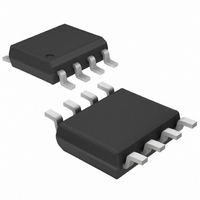
MAX883ESA+T Maxim Integrated Products, MAX883ESA+T Datasheet - Page 10

MAX883ESA+T
Manufacturer Part Number
MAX883ESA+T
Description
IC REG LINEAR 5/ADJ 200MA 8-SOIC
Manufacturer
Maxim Integrated Products
Datasheet
1.MAX882CSA.pdf
(17 pages)
Specifications of MAX883ESA+T
Regulator Topology
Positive Fixed or Adjustable
Voltage - Output
5V, 1.25 ~ 11 V
Voltage - Input
2.9 ~ 11.5 V
Voltage - Dropout (typical)
0.22V @ 200mA
Number Of Regulators
1
Current - Output
200mA
Operating Temperature
0°C ~ 70°C
Mounting Type
Surface Mount
Package / Case
8-SOIC (3.9mm Width)
Number Of Outputs
1
Polarity
Positive
Input Voltage Max
11.5 V
Output Voltage
1.25 V to 11 V, 5 V
Output Type
Adjustable, Fixed
Dropout Voltage (max)
0.22 V at 100 mA
Output Current
200 mA
Line Regulation
40 mV
Load Regulation
100 mV
Voltage Regulation Accuracy
5 %
Maximum Power Dissipation
1.5 W
Maximum Operating Temperature
+ 85 C
Mounting Style
SMD/SMT
Minimum Operating Temperature
- 40 C
Reference Voltage
1.24 V
Lead Free Status / RoHS Status
Lead free / RoHS Compliant
Current - Limit (min)
-
Lead Free Status / Rohs Status
Lead free / RoHS Compliant
5V/3.3V or Adjustable, Low-Dropout,
Low I
Figure 4. Typical Maximum Power Dissipation vs. Ground Pad
Area
The GND pins of the MAX882/MAX883/MAX884 SOIC
package perform the dual function of providing an elect-
rical connection to ground and channeling heat away. Con-
nect all GND pins to ground using a large pad or ground
plane. Where this is impossible, place a copper plane on an
adjacent layer. For a given power dissipation, the pad
should exceed the associated dimensions in Figure 4.
Figure 4 assumes the IC is in an 8-pin small-outline pack-
age that has a maximum junction temperature of +125°C
and is soldered directly to the pad; it also has a +25°C
ambient air temperature and no other heat sources. Use
larger pad sizes for other packages, lower junction tem-
peratures, higher ambient temperatures, or conditions
where the IC is not soldered directly to the heat-sinking
ground pad. When operating C- and E-grade parts up to a
T
specifications. For T
output voltage may drift more.
The MAX882/MAX883/MAX884 can regulate currents up
to 250mA and operate with input voltages up to 11.5V, but
not simultaneously. High output currents can only be sus-
tained when input-output differential voltages are small, as
shown in Figure 5. Maximum power dissipation depends
on packaging, temperature, and air flow. The maximum
output current is as follows:
where P is derived from Figure 4.
10
J
of +125°C, expect performance similar to M-grade
______________________________________________________________________________________
I
OUT(MAX)
1.6
1.5
1.4
1.3
1.2
1.1
1.0
0.9
0.0155in
0.1cm
Q
MAX883, V
8-PIN SO PACKAGE
77.4cm
SINGLE-SIDED BOARD
1oz COPPER
GLASS EPOXY,
T
T
, 200mA Linear Regulators
J
A
2
2
= +125°C,
= +25°C, STILL AIR
J
2
,
COPPER GROUND PAD AREA
between +125°C and +150°C, the
=
0.155in
OUT
1cm
(V
= 5V
IN
2
2
P(T
−
V
OUT
J
1.55in
10cm
−
T )
)100 C
A
2
2
°
100cm
15.5in
2
2
Figure 5a. Safe Operating Regions: MAX882/MAX884 Maximum
Output Current vs. Supply Voltage
Figure 5b. Safe Operating Regions: MAX883 Maximum Output
Current vs. Supply Voltage
250
250
200
150
100
200
150
100
50
50
0
0
2
4
MAXIMUM CURRENT
MAXIMUM CURRENT
3
5
4
PLASTIC DIP
OPERATING
REGION AT
T A = +25°C
T J = +125°C
6
OPERATING
REGION AT
T A = +25°C
T J = +125°C
PLASTIC DIP
5
SUPPLY VOLTAGE (V)
SUPPLY VOLTAGE (V)
CERAMIC DIP
7
6
CERAMIC DIP
7
8
8
MAXIMUM POWER
DISSIPATION LIMIT
9
MAXIMUM POWER
DISSIPATION LIMIT
POWER
HIGH-
9
SOIC
10
POWER
HIGH-
10
SOIC
11
11
12
12
13
13


