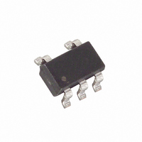
MAX8878EUK33+T Maxim Integrated Products, MAX8878EUK33+T Datasheet - Page 7

MAX8878EUK33+T
Manufacturer Part Number
MAX8878EUK33+T
Description
IC REG LINEAR 150MA SOT23-5
Manufacturer
Maxim Integrated Products
Datasheet
1.MAX8878EZK30T.pdf
(10 pages)
Specifications of MAX8878EUK33+T
Regulator Topology
Positive Fixed
Voltage - Output
3.3V
Voltage - Input
Up to 6.5V
Voltage - Dropout (typical)
0.165V @ 150mA
Number Of Regulators
1
Current - Output
150mA (Min)
Current - Limit (min)
160mA
Operating Temperature
-40°C ~ 85°C
Mounting Type
Surface Mount
Package / Case
SOT-23-5, SC-74A, SOT-25
Lead Free Status / RoHS Status
Lead free / RoHS Compliant
The MAX8877/MAX8878 are supplied with factory-set
output voltages from 1.5V to 5.0V, in 100mV increments.
Except for the MAX887_EUK29 and the MAX887_EUK32
(which have an output voltage preset at 2.84V and
3.15V, respectively), the two-digit suffix allows the cus-
tomer to choose the output voltage in 100mV increments.
For example, the MAX8877EUK33 has a preset output
voltage of 3.3V (see Expanded Ordering Information).
The MAX8877/MAX8878 feature a 1.1Ω typical
P-channel MOSFET pass transistor. This provides sever-
al advantages over similar designs using PNP pass tran-
sistors, including longer battery life. The P-channel
MOSFET requires no base drive, which reduces quies-
cent current considerably. PNP-based regulators waste
considerable current in dropout when the pass transistor
saturates. They also use high base-drive currents under
large loads. The MAX8877/MAX8878 do not suffer from
these problems and consume only 100µA of quiescent
current whether in dropout, light-load, or heavy-load
applications (see the Typical Operating Characteristics).
The MAX8877/MAX8878 include a current limiter, which
monitors and controls the pass transistor’s gate voltage,
limiting the output current to 390mA. For design purposes,
consider the current limit to be 160mA minimum to 500mA
maximum. The output can be shorted to ground for an
indefinite amount of time without damaging the part.
Thermal-overload protection limits total power dissipa-
tion in the MAX8877/MAX8878. When the junction tem-
perature exceeds T
signals the shutdown logic, turning off the pass transis-
tor and allowing the IC to cool. The thermal sensor will
turn the pass transistor on again after the IC’s junction
temperature cools by 15°C, resulting in a pulsed output
during continuous thermal-overload conditions.
Thermal-overload protection is designed to protect the
MAX8877/MAX8878 in the event of fault conditions. For
continual operation, do not exceed the absolute maxi-
mum junction-temperature rating of T
The MAX8877/MAX8878’s maximum power dissipation
depends on the thermal resistance of the case and circuit
board, the temperature difference between the die junc-
tion and ambient air, and the rate of air flow. The power
dissipation across the device is P = I
The maximum power dissipation is:
Operating Region and Power Dissipation
Internal P-Channel Pass Transistor
Thermal-Overload Protection
_______________________________________________________________________________________
Low-Noise, Low-Dropout, 150mA Linear
J
= +155°C, the thermal sensor
Output Voltage
J
OUT
Current Limit
= +150°C.
(V
IN
Regulators with '2982 Pinout
- V
OUT
).
where T
the MAX8877/MAX8878 die junction and the surround-
ing air, θ
package, and θ
printed circuit board, copper traces, and other materi-
als to the surrounding air.
The GND pin of the MAX8877/MAX8878 performs the
dual function of providing an electrical connection to
ground and channeling heat away. Connect the GND
pin to ground using a large pad or ground plane.
The MAX8877/MAX8878 have a unique protection
scheme that limits the reverse supply current to 1mA
when either V
cuitry monitors the polarity of these two pins and discon-
nects the internal circuitry and parasitic diodes when the
battery is reversed. This feature prevents device damage.
An external 0.01µF bypass capacitor at BP, in conjunc-
tion with an internal 200kΩ resistor, creates a 80Hz low-
pass filter for noise reduction. The MAX8877/MAX8878
exhibit 30µV
0.01µF and C
applications. Start-up time is minimized by a power-on
circuit that pre-charges the bypass capacitor. The
Typical Operating Characteristics section shows
graphs of Noise vs. BP Capacitance, Noise vs. Load
Current, and Output Noise Spectral Density.
Normally, use a 1µF capacitor on the MAX8877/
MAX8878’s input and a 1µF to 10µF capacitor on the out-
put. Larger input capacitor values and lower ESRs pro-
vide better supply-noise rejection and line-transient
response. Reduce noise and improve load-transient
response, stability, and power-supply rejection by using
large output capacitors. For stable operation over the full
temperature range and with load currents up to 150mA, a
1µF (min) ceramic capacitor is recommended for V
2.5V and 3.3µF and for V
Note that some ceramic dielectrics exhibit large capaci-
tance and ESR variation with temperature. With
dielectrics such as Z5U and Y5V, it may be necessary to
increase the capacitance by a factor of 2 or more to
ensure stability at temperatures below -10°C. With X7R or
X5R dielectrics, 1µF should be sufficient at all operating
temperatures for V
____________Applications Information
J
JB
- T
P
(or θ
RMS
A
IN
MAX
OUT
is the temperature difference between
BA
or V
JC
of output voltage noise with C
OUT
is the thermal resistance through the
= (T
= 10µF. This is negligible in most
Reverse Battery Protection
) is the thermal resistance of the
SHDN
≥ 2.5V. A graph of the Region of
J
OUT
Capacitor Selection and
- T
falls below ground. Their cir-
A
< 2.5V.
) / (θ
Regulator Stability
JB
Noise Reduction
+ θ
BA
)
OUT
BP
=
7
≥


