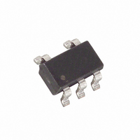
MAX1735EUK30+T Maxim Integrated Products, MAX1735EUK30+T Datasheet - Page 8

MAX1735EUK30+T
Manufacturer Part Number
MAX1735EUK30+T
Description
IC REG LDO NEG OUT 200MA SOT23-5
Manufacturer
Maxim Integrated Products
Datasheet
1.MAX1735EUK25-T.pdf
(10 pages)
Specifications of MAX1735EUK30+T
Regulator Topology
Negative Fixed or Adjustable
Voltage - Output
-3V, -1.25 ~ -5.5 V
Voltage - Input
-2.5 ~ -6.5 V
Voltage - Dropout (typical)
0.08V @ 200mA
Number Of Regulators
1
Current - Output
200mA (Min)
Current - Limit (min)
1.02A
Operating Temperature
-40°C ~ 85°C
Mounting Type
Surface Mount
Package / Case
SOT-23-5, SC-74A, SOT-25
Number Of Outputs
1
Polarity
Negative
Input Voltage Max
- 6.5 V
Output Voltage
- 1.25 V to - 5.5 V, - 3 V
Output Type
Adjustable, Fixed
Dropout Voltage (max)
0.24 V at - 200 mA
Output Current
200 mA
Line Regulation
0 % / V
Load Regulation
0.004 % / mA
Voltage Regulation Accuracy
1 %
Maximum Power Dissipation
0.571 W
Maximum Operating Temperature
+ 85 C
Mounting Style
SMD/SMT
Minimum Operating Temperature
- 40 C
Reference Voltage
- 1.25 V
Lead Free Status / RoHS Status
Lead free / RoHS Compliant
Maximum power dissipation of the MAX1735 depends
on the thermal resistance of the case and the circuit
board, the temperature difference between the die
junction and ambient air, and the rate of air flow (see
also Thermal Overload Protection). The maximum
power that can be dissipated by the device is:
where the numerator expresses the temperature differ-
ence between the maximum allowed die junction
(+150°C) and the surrounding air, θ
is the thermal resistance of the package, and θ
to ambient) is the thermal resistance from the package
through the PC board, traces, and other material to the
surrounding air. The former is a characteristic solely of
the device in its package, and the latter is completely
defined by PC board layout and airflow. It is important to
note that the ability to dissipate power is as much a func-
tion of the PC board layout and air flow as the packaged
part itself. Hence, a manufacturer can reliably provide a
value for θ
total thermal resistance θ
θ
the thermal characteristics of the application circuit.
Figure 4 shows the estimated allowable power dissipa-
tion for a MAX1735 mounted on a typical PC board at
ambient temperatures of +50°C, +70°C, and +85°C.
Figure 4 shows the maximum continuous output current
for a particular input-to-output voltage differential, for
200mA, Negative-Output, Low-Dropout
Linear Regulator in SOT23
Figure 4. Output Current and In-Out Voltage Differential
Operating Region Bounded by Available Power Dissipation at
Selected Ambient Temperatures
8
CA
Operating Region and Power Dissipation
, and the manufacturer can seldom reliably predict
_______________________________________________________________________________________
P
JC
MAX
250
200
150
100
50
, but not accurately provide a value for the
0
vs. INPUT-OUTPUT VOLTAGE DIFFERENTIAL
0
=
INPUT-OUTPUT VOLTAGE DIFFERENTIAL (V)
T
MAXIMUM CONTINUOUS CURRENT
θ
MAXIMUM OUTPUT CURRENT
JMAX
JC
1
AT MAXIMUM
JUNCTION TEMP
(T
J
+
= +150°C)
θ
2
−
JA
CA
T
A
. θ
3
=
JA
T
JMAX
is the sum of θ
4
θ
JC
JA
−
(junction to case)
5
T
A
6
CA
JC
(case
and
selected ambient temperatures. The working principle is
that the SOT23-5 package is small enough that in a typi-
cal application circuit at room temperature, the package
cannot dissipate enough power to allow -6.5V to be reg-
ulated to -1.25V at -200mA output (more than 1200mW).
As ambient temperature falls, the available power dissi-
pation increases to allow for a greater operating region.
The equation for the family of curves follows:
where
is the absolute maximum rated power dissipation at
+70°C for the SOT23-5, and θ
approximate junction-to-ambient thermal resistance of
the SOT23-5 in a typical application.
A key to reducing θ
ductivity to the PC board, is to provide large PC board
pads and traces for IN.
Capacitors are required at the input and output of the
MAX1735. Connect a 1µF or greater capacitor between
IN and GND. This input capacitor serves only to lower
the source impedance of the input supply in transient
conditions; a smaller value can be used when the regu-
lator is powered from a low-impedance source, such as
another regulated supply or low-impedance batteries.
For output voltages between -2.5V and -5.5V, connect
a 1µF or greater capacitor between OUT and GND. For
voltages between -1.25V and -2.5V, use a 2.2µF or
greater output capacitor. The maximum value of the
output capacitor to guarantee stability is 10µF.
The output capacitor’s value and equivalent series
resistance (ESR) affect stability and output noise. To
ensure stability and optimum transient response, output
capacitor ESR should be 0.1Ω or less for output volt-
ages from -1.25V to -2.45V and 0.2Ω or less for output
voltages between -2.5V and -5.5V. Inexpensive sur-
face-mount ceramic capacitors typically have very-low
ESR and are commonly available in values up to 10µF.
Other low-ESR capacitors, such as surface-mount tan-
talum, may also be used. Do not use low-cost alu-
minum electrolytic capacitors due to their large size
and relatively high ESR. Lastly, make sure the input and
output capacitors are as close to the IC as possible to
minimize the impact of PC board trace impedance.
__________Applications Information
|
I
OUT
|
is in mA,
|
I
OUT
|
CA
=
, thereby increasing thermal con-
P
|
V
MAX
|
V
Capacitor Selection and
OUT
OUT
−
- V
T
−
A
θ
Regulator Stability
JA
V
IN
JA
−
IN
|
70
(0.140°C/mW) is the
|
in V, P
MAX
(571mW)


