P40-G240-WH Bourns Inc., P40-G240-WH Datasheet - Page 4
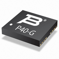
P40-G240-WH
Manufacturer Part Number
P40-G240-WH
Description
SURGE SUPP TBU 240MA 40VIMP SMD
Manufacturer
Bourns Inc.
Series
TBU™r
Specifications of P40-G240-WH
Voltage - Working
28V
Technology
Mixed Technology
Number Of Circuits
2
Applications
General Purpose
Package / Case
0.157" L x 0.157" W x 0.033" H (4.00mm x 4.00mm x 0.85mm)
Voltage Rating
40 V
Current Rating
240 mA
Height
0.85 mm
Length
4 mm
Mounting
SMD/SMT
Operating Temperature Range
- 40 C to + 85 C
Termination Style
SMD/SMT
Width
4 mm
Suppressor Type
Data Line / Mains
Output Current
480mA
Peak Surge Current
240mA
Response Time
200ns
Resistance
3.6ohm
Operating Temperature Max
85°C
Clamping Voltage Vc Max
40V
Length/height, External
0.85mm
Rohs Compliant
Yes
External Depth
4mm
External Width
4mm
Lead Free Status / RoHS Status
Lead free / RoHS Compliant
Power (watts)
-
Voltage - Clamping
-
Lead Free Status / Rohs Status
Lead free / RoHS Compliant


TBU
mask defi ne (NSMD). Recommended stencil thickness is 0.10-0.12 mm (.004-.005 in.) with
stencil opening size 0.025 mm (.0010 in.) less than the device pad size. As when heat sink-
ing any power device, it is recommended that, wherever possible, extra PCB copper area is
allowed. For minimum parasitic capacitance, do not allow any signal, ground or power
signals beneath any of the pads of the device.
Thermal resistance using minimal pad size, where the power is the total power dissipated in the package. Additional copper pad area to be
used for additional heatsinking is also recommended.
Thermal Resistances
Product Dimensions
Recommended Pad Layout
Symbol
A
R
R
®
TBU
th(j-a)
th(j-a)
devices have matte-tin termination fi nish. Suggested layout should use non-solder
(.035)
(.014)
0.90
(.012)
0.35
0.30
®
TOP VIEW
P40-G Protectors
Parameter
Junction to Package Pads (1 TBU of Pair)
Junction to Package Pads (2 TBUs of Equal Power)
PIN 1
B
(.012 +.002/-.000)
0.30 +0.05/-0.00
(.102)
2.60
C
SIDE VIEW
D
(.057)
1.45
NC = Solder to PCB; do not make electrical
connection, do not connect to ground.
F
G
G
K
4
3
Pad #
J
1
2
3
4
5
6
BOTTOM VIEW
Pad Designation
5
2
E
K
J
6
1
Apply
Out1
Out2
Customers should verify actual device performance in their specifi c applications.
In1
NC
NC
In2
H
H
F
M
N
N
Block Diagram
Dim.
Specifi cations are subject to change without notice.
G
M
A
B
C
D
E
H
K
N
F
J
DIMENSIONS:
Value
(.154)
(.154)
(.031)
0.000
(.000)
(.100)
(.008)
(.030)
(.055)
(.004)
(.010)
(.022)
(.008)
6
1
Min.
3.90
0.80
0.20
0.75
1.40
0.10
0.25
0.55
0.20
3.90
2.55
180
250
TBU™ Device
0.025
(.157)
(.157)
(.033)
(.001)
(.102)
(.010)
(.031)
(.057)
(.006)
(.012)
(.024)
(.010)
(INCHES)
Typ.
4.00
0.85
2.60
0.25
0.80
1.45
0.15
0.30
0.60
0.25
4.00
MM
4
3
°C/W
°C/W
Unit
(.161)
(.161)
(.035)
0.050
(.002)
(.104)
(.012)
(.033)
(.059)
(.008)
(.014)
(.026)
(.012)
Max.
4.10
4.10
0.90
2.65
0.30
0.85
1.50
0.20
0.35
0.65
0.30
Related parts for P40-G240-WH
Image
Part Number
Description
Manufacturer
Datasheet
Request
R

Part Number:
Description:
Definite Purpose Magnetic Contactor
Manufacturer:
Tyco
Datasheet:

Part Number:
Description:
Tbu P40-g Protectors
Manufacturer:
Bourns, Inc.
Datasheet:

Part Number:
Description:
CONTACTOR 40A 3PST 24VDC
Manufacturer:
Tyco Electronics
Datasheet:

Part Number:
Description:
RELAY CONTACTOR 40A 3PST 12VDC
Manufacturer:
Tyco Electronics
Datasheet:

Part Number:
Description:
CONTACTOR 24VDC 40A MAG 4PST
Manufacturer:
Tyco Electronics
Datasheet:

Part Number:
Description:
CONTACTOR 24VDC 40A MAG 3PST
Manufacturer:
Tyco Electronics
Datasheet:
Part Number:
Description:
RELAY CONTACTOR 40A 3PST 120VDC
Manufacturer:
Tyco Electronics
Datasheet:
Part Number:
Description:
RELAY CONTACTOR 40A 3PST 24VAC
Manufacturer:
Tyco Electronics
Datasheet:
Part Number:
Description:
RELAY CONTACTOR 40A 3PST 120VAC
Manufacturer:
Tyco Electronics
Datasheet:
Part Number:
Description:
RELAY CONTACTOR 40A 3PST 240VAC
Manufacturer:
Tyco Electronics
Datasheet:
Part Number:
Description:
RELAY CONTACTOR 40A DPST 12VDC
Manufacturer:
Tyco Electronics
Datasheet:
Part Number:
Description:
RELAY CONTACTOR 40A DPST 24VDC
Manufacturer:
Tyco Electronics
Datasheet:
Part Number:
Description:
P40C43A12C1-120=CONTACTOR ASSEMBLY
Manufacturer:
Tyco Electronics
Datasheet:

Part Number:
Description:
P40P47D14P1-24=CONTACTORS
Manufacturer:
Tyco Electronics
Datasheet: