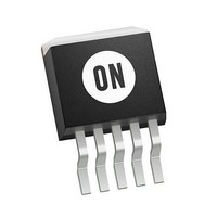
NCP5662DS33R4G ON Semiconductor, NCP5662DS33R4G Datasheet

NCP5662DS33R4G
Specifications of NCP5662DS33R4G
NCP5662DS33R4GOSTR
Available stocks
Related parts for NCP5662DS33R4G
NCP5662DS33R4G Summary of contents
Page 1
NCP5662, NCV5662 Low Output Voltage, Ultra-Fast 2.0 A Low Dropout Linear Regulator with Enable The NCP5662/NCV5662 is a high performance, low dropout linear regulator designed for high power applications that require up to 2.0 A current offered in ...
Page 2
NCP5662 NCV5662 EN EF GND C in Enable OFF ON Figure 1. Typical Application Schematic, Fixed Output PIN FUNCTION DESCRIPTION Pin Pin Adj/Fixed Adj/Fixed 2 D PAK DFN8 TAB ...
Page 3
V in Voltage Reference V = 0.9 V ref Block R3 Output Stage R4 Error Flag Figure 3. Block Diagram, Fixed Output V in Voltage Reference V = 0.9 V Block ref R3 Output Stage R4 GND Figure 4. Block ...
Page 4
ABSOLUTE MAXIMUM RATINGS Rating Input Voltage (Note 1) Output Pin Voltage Adjust Pin Voltage Enable Pin Voltage Error Flag Voltage Error Flag Current Maximum Junction Temperature Stresses exceeding Maximum Ratings may damage the device. Maximum Ratings are stress ratings only. ...
Page 5
ELECTRICAL CHARACTERISTICS version −40°C to 125°C (NCV version Characteristic ADJUSTABLE OUTPUT VERSION Output Noise Voltage Output Voltage T = 25° +1 7 out T = −20 to ...
Page 6
ELECTRICAL CHARACTERISTICS version −40°C to 125°C (NCV version Characteristic FIXED OUTPUT VOLTAGE Output Noise Voltage (V = 0.9 V) out Output Voltage (Note 25° +1 7 ...
Page 7
Figure 5. Dropout Voltage vs. Temperature 1 1.5 V Fixed out C = 150 mF in ...
Page 8
out 0 150 1.0 to 150 mF 0.2 out T = 25° 1.0 2.0 3.0 4.0 5.0 6 INPUT VOLTAGE ...
Page 9
0.9 V out out 150 150 mF 10 out T = 25° ...
Page 10
1.5 V Fixed out C = 150 150 mF out T = 25° 2.0 A out TIME (1.0 ms/Div) Figure 18. Load Transient ...
Page 11
The NCP5662 is a high performance low dropout 2.0 A linear regulator suitable for high power applications, featuring an ultra−fast response time and low noise without a bypass capacitor offered in both fixed and adjustable output versions with ...
Page 12
Copper Copper 40 0 100 200 300 400 COPPER AREA (mm Figure 25. DFN8 Thermal Resistance vs. Copper Area NCP5662 Evaluation Board Figure 26. Test Board used for Evaluation ...
Page 13
... ORDERING INFORMATION Device NCP5662DSADJR4G NCP5662DS12R4G NCP5662DS15R4G NCP5662DS18R4G NCP5662DS25R4G NCP5662DS28R4G NCP5662DS30R4G NCP5662DS33R4G NCV5662DSADJR4G NCV5662DS15R4G NCP5662MNADJR2G NCP5662MN15R2G NCP5662MN33R2G †For information on tape and reel specifications, including part orientation and tape sizes, please refer to our Tape and Reel Packaging Specifications Brochure, BRD8011/D. Nominal Output Voltage ...
Page 14
... 10.66 0.42 *For additional information on our Pb−Free strategy and soldering details, please download the ON Semiconductor Soldering and Mounting Techniques Reference Manual, SOLDERRM/D. PACKAGE DIMENSIONS 2 D PAK 5−LEAD CASE 936AA−01 ISSUE −A− SOLDERING FOOTPRINT* 8.38 0.33 3.05 0.12 16.02 0.63 SCALE 3:1 http://onsemi ...
Page 15
... NOTE 3 0.05 C *For additional information on our Pb−Free strategy and soldering details, please download the ON Semiconductor Soldering and Mounting Techniques Reference Manual, SOLDERRM/D. N. American Technical Support: 800−282−9855 Toll Free USA/Canada Europe, Middle East and Africa Technical Support: Phone: 421 33 790 2910 Japan Customer Focus Center Phone: 81− ...


