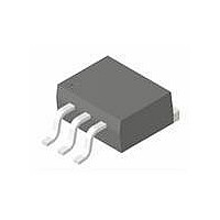
NCP565D2TR4G ON Semiconductor, NCP565D2TR4G Datasheet - Page 12

NCP565D2TR4G
Manufacturer Part Number
NCP565D2TR4G
Description
IC REG LDO 1.5A ADJ D2PAK-5
Manufacturer
ON Semiconductor
Datasheet
1.NCP565V12EVB.pdf
(17 pages)
Specifications of NCP565D2TR4G
Regulator Topology
Positive Adjustable
Voltage - Output
0.9 ~ 7.7 V
Voltage - Input
2.5 ~ 9 V
Voltage - Dropout (typical)
0.9V @ 1.5A
Number Of Regulators
1
Current - Output
1.5A
Current - Limit (min)
1.6A
Operating Temperature
-40°C ~ 125°C
Mounting Type
Surface Mount
Package / Case
TO-263-5, D²Pak (5 leads + Tab), TO-263BA
Number Of Outputs
1
Polarity
Positive
Input Voltage Max
9 V
Output Voltage
0.9 V to 7.7 V
Output Type
Adjustable
Dropout Voltage (max)
1.3 V at 1500 mA
Output Current
1.5 A
Line Regulation
0.03 %
Load Regulation
0.03 %
Voltage Regulation Accuracy
3 %
Maximum Operating Temperature
+ 125 C
Mounting Style
SMD/SMT
Minimum Operating Temperature
- 40 C
Reference Voltage
0.927 V
Lead Free Status / RoHS Status
Lead free / RoHS Compliant
Other names
NCP565D2TR4GOS
NCP565D2TR4GOS
NCP565D2TR4GOSTR
NCP565D2TR4GOS
NCP565D2TR4GOSTR
Available stocks
Company
Part Number
Manufacturer
Quantity
Price
Company:
Part Number:
NCP565D2TR4G
Manufacturer:
ON Semiconductor
Quantity:
1 799
Part Number:
NCP565D2TR4G
Manufacturer:
ON/安森美
Quantity:
20 000
Protection Diodes
regulator it is sometimes necessary to add protection diodes.
If the input voltage of the regulator gets shorted, the output
capacitor will discharge into the output of the regulator. The
discharge current depends on the value of the capacitor, the
output voltage and the rate at which V
NCP565 linear regulator, the discharge path is through a
large junction and protection diodes are not usually needed.
If the regulator is used with large values of output
capacitance and the input voltage is instantaneously shorted
to ground, damage can occur. In this case, a diode connected
as shown in Figure 24 is recommended.
When large external capacitors are used with a linear
V
Figure 24. Protection Diode for Large
in
C
1
V
GND
in
Output Capacitors
1N4002 (Optional)
NCP565
V
Adj
out
C
Adj
R
R
in
1
2
drops. In the
C
V
out
2
http://onsemi.com
12
Thermal Considerations
that is designed to protect the regulator in the event that the
maximum junction temperature is exceeded. This feature
provides protection from a catastrophic device failure due to
accidental overheating. It is not intended to be used as a
substitute for proper heat sinking. The maximum device
power dissipation can be calculated by:
This series contains an internal thermal limiting circuit
200
180
160
140
120
100
80
60
40
0
50 100 150
COPPER HEAT−SPREADER AREA (mm sq)
Figure 25. Thermal Resistance
DFN 1 oz Cu
P D +
DFN 2 oz Cu
T J(max) * T A
200 250 300 350 400 450 500
SOT−223 1 oz Cu
R qJA
SOT−223 2 oz Cu
D
2
D
PAK 1 oz Cu
2
PAK 2 oz Cu


