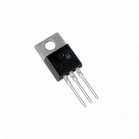
MC7912BTG ON Semiconductor, MC7912BTG Datasheet - Page 5

MC7912BTG
Manufacturer Part Number
MC7912BTG
Description
IC REG NEG VOLT 1A 12V TO220AB
Manufacturer
ON Semiconductor
Type
Linearr
Datasheet
1.MC7915CTG.pdf
(16 pages)
Specifications of MC7912BTG
Regulator Topology
Negative Fixed
Voltage - Output
-12V
Voltage - Input
Down to -35V
Voltage - Dropout (typical)
1.3V @ 1A
Number Of Regulators
1
Current - Output
1A
Operating Temperature
-40°C ~ 125°C
Mounting Type
Through Hole
Package / Case
TO-220-3 (Straight Leads)
Package
3TO-220
Function
Standard
Number Of Outputs
1
Output Voltage
-12 V
Maximum Output Current
1 A
Output Type
Fixed
Accuracy
±4 %
Typical Dropout Voltage @ Current
1.3@1A V
Polarity
Negative
Output Current
1 A
Line Regulation
240 mV
Load Regulation
240 mV
Input Voltage Max
- 35 V
Maximum Operating Temperature
+ 125 C
Minimum Operating Temperature
- 40 C
Mounting Style
Through Hole
Voltage Regulation Accuracy
4 %
Lead Free Status / RoHS Status
Lead free / RoHS Compliant
Current - Limit (min)
-
Lead Free Status / Rohs Status
Lead free / RoHS Compliant
Other names
MC7912BTG
MC7912BTGOS
MC7912BTGOS
Available stocks
Company
Part Number
Manufacturer
Quantity
Price
Company:
Part Number:
MC7912BTG
Manufacturer:
ON
Quantity:
5 600
Company:
Part Number:
MC7912BTG
Manufacturer:
ON
Quantity:
3 400
Part Number:
MC7912BTG
Manufacturer:
ON/安森美
Quantity:
20 000
4. Load and line regulation are specified at constant junction temperature. Changes in V
*Tlow = −40°C for MC7912B and Tlow = 0°C for MC7912C.
MC7912B, MC7912C
ELECTRICAL CHARACTERISTICS
MC7912AC
ELECTRICAL CHARACTERISTICS
Output Voltage (T
Line Regulation (Note 4)
Load Regulation, T
Output Voltage
Input Bias Current (T
Input Bias Current Change
Output Noise Voltage (T
Ripple Rejection (I
Dropout Voltage (I
Average Temperature Coefficient of Output Voltage
Output Voltage (T
Line Regulation (Note 4)
Load Regulation (Note 4)
Output Voltage
Input Bias Current
Input Bias Current Change
Output Noise Voltage (T
Ripple Rejection (I
Dropout Voltage (I
Average Temperature Coefficient of Output Voltage
separately. Pulse testing with low duty cycle is used.
(T
(T
5.0 mA ≤ I
250 mA ≤ I
−14.5 Vdc ≥ V
−14.5 Vdc ≥ V
5.0 mA ≤ I
I
−16 Vdc ≥ V
−16 Vdc ≥ V
−14.8 Vdc ≥ V
−14.5 Vdc ≥ V
5.0 mA ≤ I
250 mA ≤ I
5.0 mA ≤ I
−14.8 Vdc ≥ V
−15 Vdc ≥ V
5.0 mA ≤ I
5.0 mA ≤ I
I
O
O
J
J
−14.5 Vdc ≥ V
−16 Vdc ≥ V
−14.5 Vdc ≥ V
−16 Vdc ≥ V
= 5.0 mA, Tlow* ≤ T
= 5.0 A, Tlow* ≤ T
= +25°C, I
= +25°C, I
O
O
O
O
O
O
O
O
≤ 1.5 A
≤ 1.5 A
I
I
≤ 1.5 A, T
≤ 1.0 A
I
≤ 1.0 A
≤ 1.5 A, T
≤ 750 mA
≤ 750 mA
≥ − 22 Vdc; I
≥ − 22 Vdc; I
≥ − 30 Vdc
O
O
I
I
I
I
I
I
I
≥ − 27 Vdc, 5.0 mA ≤ I
≥ − 30 Vdc
≥ − 30 Vdc; I
≥ − 27 Vdc; I
≥ − 27 Vdc, 5.0 mA ≤ I
J
J
≥ − 22 Vdc
≥ − 22 Vdc
= 100 mA)
= 500 mA)
O
O
O
O
I
I
J
= +25°C)
= +25°C)
≥ − 30 Vdc
≥ − 30 Vdc
= 1.0 A, T
= 1.0 A, T
= +25°C (Note 4)
= 20 mA, f = 120 Hz)
= 20 mA, f = 120 Hz)
J
= +25°C)
J
A
A
J
J
≤ +125°C
J
= +25°C, 10 Hz ≤ f ≤ 100 kHz)
= +25°C, 10 Hz ≤ f ≤ 100 kHz)
= +25°C
= +25°C
≤ +125°C
O
O
O
O
= 1.0 A, T
= 1.0 A
J
J
= +25°C)
= +25°C)
= 500 mA
= 1.0 A, T
Characteristics
Characteristics
O
O
J
(V
(V
= +25°C
≤ 1.0 A, P ≤ 15 W
≤ 1.0 A, P ≤ 15 W
J
I
I
= +25°C
= −19 V, I
= −19 V, I
O
O
= 500 mA, Tlow* < T
= 500 mA, Tlow* < T
http://onsemi.com
5
J
J
< +125°C, unless otherwise noted.)
< +125°C, unless otherwise noted.)
Symbol
DV
Symbol
DV
Reg
Reg
Reg
Reg
O
V
V
DI
DI
RR
RR
V
V
I
V
V
I
due to heating effects must be taken into account
I
V
I
V
−V
O
−V
O
IB
IB
O
O
O
O
load
IB
n
load
IB
n
/DT
/DT
line
line
O
O
−11.75
−11.5
−11.4
−11.5
Min
Min
−
−
−
−
−
−
−
−
−
−
−
−
−
−
−
−
−
−
−
−
−
−
−
−
−
−
−
−
−1.0
−1.0
Typ
Typ
−12
−12
6.0
4.4
1.3
6.0
4.4
1.3
13
55
24
46
17
75
61
24
24
13
46
17
35
75
61
−
−
−
−
−
−
−
−12.25
−12.5
−12.6
−12.5
Max
Max
120
240
120
240
120
120
120
120
150
150
8.0
1.0
0.5
8.0
0.8
0.5
0.5
60
60
75
−
−
−
−
−
−
−
−
mV/°C
mV/°C
Unit
Unit
Vdc
Vdc
Vdc
Vdc
Vdc
Vdc
mV
mV
mA
mA
mV
mV
mA
mA
dB
dB
mV
mV


