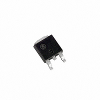
MC33275DT-3.0G ON Semiconductor, MC33275DT-3.0G Datasheet - Page 4

MC33275DT-3.0G
Manufacturer Part Number
MC33275DT-3.0G
Description
IC REG LDO 300MA 3V DPAK
Manufacturer
ON Semiconductor
Datasheet
1.MC33275MN-3.3R2G.pdf
(15 pages)
Specifications of MC33275DT-3.0G
Regulator Topology
Positive Fixed
Voltage - Output
3V
Voltage - Input
Up to 13V
Voltage - Dropout (typical)
0.26V @ 300mA
Number Of Regulators
1
Current - Output
300mA (Max)
Operating Temperature
-40°C ~ 125°C
Mounting Type
Surface Mount
Package / Case
TO-252-2, DPak (2 Leads + Tab), TO-252AA, SC-63
Number Of Outputs
1
Polarity
Positive
Input Voltage Max
13 V
Output Voltage
3 V
Output Type
Fixed
Dropout Voltage (max)
0.1 V at 10 mA
Output Current
300 mA
Line Regulation
10 mV
Load Regulation
25 mV
Voltage Regulation Accuracy
1 %
Maximum Operating Temperature
+ 125 C
Mounting Style
SMD/SMT
Minimum Operating Temperature
- 40 C
Lead Free Status / RoHS Status
Lead free / RoHS Compliant
Current - Limit (min)
-
Lead Free Status / Rohs Status
Details
Available stocks
Company
Part Number
Manufacturer
Quantity
Price
Company:
Part Number:
MC33275DT-3.0G
Manufacturer:
ON Semiconductor
Quantity:
135
Company:
Part Number:
MC33275DT-3.0G
Manufacturer:
ON Semiconductor
Quantity:
500
change in load current at constant chip temperature.
the regulator output no longer maintains regulation against
further reductions in input voltage. Measured when the
output drops 100 mV below its nominal value (which is
measured at 1.0 V differential), dropout voltage is affected
by junction temperature, load current and minimum input
supply requirements.
output with a constant load and no input ripple, measured
over a specified frequency range.
dissipation for which the regulator will operate within
specifications.
regulator chip and is not delivered to the load.
change in the input voltage. The measurement is made under
conditions of low dissipation or by using pulse techniques
such that the average chip temperature is not significantly
affected.
package power dissipation is the power dissipation level at
which the junction temperature reaches its maximum value
i.e. 150°C. The junction temperature is rising while the
Load Regulation − The change in output voltage for a
Dropout Voltage − The input/output differential at which
Output Noise Voltage − The RMS AC voltage at the
Maximum Power Dissipation − The maximum total
Quiescent Current − Current which is used to operate the
Line Regulation − The change in output voltage for a
Maximum Package Power Dissipation − The maximum
http://onsemi.com
DEFINITIONS
4
difference between the input power (V
output power (V
calculate the maximum power dissipation and so the
maximum current as following:
specified at 150°C, if T
neglecting the quiescent current, the maximum power
dissipation can be expressed as:
evaluated by deliberately activating the thermal shutdown
of the circuit (by increasing the output current or raising the
input voltage for example).
subtracting the output power from the input power. All
variables are then well known: power dissipation, thermal
shutdown temperature and ambient temperature.
Depending on ambient temperature, it is possible to
The maximum operating junction temperature T
The thermal resistance of the whole circuit can be
Then you can calculate the power dissipation by
Pd +
I out +
R
qJA
out
X I
T
R
+
J
V
qJA
CC
T
out
T
A
J
P
A
P
D
D
= 25°C, then P
) is increasing.
T
V out
A
CC
D
can be found. By
X I
CC
) and the
J
is


