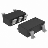
MC33761SNT1-050G ON Semiconductor, MC33761SNT1-050G Datasheet

MC33761SNT1-050G
Specifications of MC33761SNT1-050G
MC33761SNT1-050GOS
MC33761SNT1-050GOSTR
Available stocks
Related parts for MC33761SNT1-050G
MC33761SNT1-050G Summary of contents
Page 1
MC33761 Ultra Low−Noise Low Dropout Voltage Regulator with 1.0 V ON/OFF Control The MC33761 is an Low DropOut (LDO) regulator featuring excellent noise performances. Thanks to its innovative design, the circuit reaches an impressive 40 mVRMS noise level without an ...
Page 2
PIN FUNCTION DESCRIPTIONS Pin # Pin Name Function 1 V Powers the GND The IC’s ground 3 ON/OFF Shuts or wakes−up the None 5 V Delivers the output voltage out MAXIMUM RATINGS Rating Power ...
Page 3
ELECTRICAL CHARACTERISTICS (continued) (For typical values T = 25°C, for min/max values T A Characteristics OUTPUT VOLTAGES V + 1.0 V < V < 6 25°C, 1.0 mA < I out in A 2.5 V 2.8 V ...
Page 4
Load Regulation The change in output voltage for a change in output current at a constant chip temperature. Dropout Voltage The input/output differential at which the regulator output no longer maintains regulation against further reductions in input voltage. Measured when ...
Page 5
All curves taken with V 4.5 4.0 3.5 3.0 2.5 2.0 1.5 1.0 0 OUTPUT CURRENT (mA) Figure 2. Ground Current versus Output Current 200 150 100 OUTPUT CURRENT ...
Page 6
... Vin max + output current is needed, the ground current is extracted from the data−sheet curves: 4 mA. For a MC33761SNT1−28 (2.8 V) delivering 80 mA and operating at 25°C, the maximum input voltage will then be 8.3 V. Typical Applications The following picture portrays the typical application of the MC33761 ...
Page 7
Input Permanently Enables the IC When Closed + for any low noise designs, particular care has to be taken when tackling Printed Circuit Board (PCB) layout. The figure below gives an example of a layout where ...
Page 8
Understanding the Load Transient Improvement The MC33761 features a novel architecture which allows the user to easily implement the regulator in burst systems where the time between two current shots is kept very small. The quality of the transient response ...
Page 9
Thanks to the lack of bypass capacitor the MC33761 is able to supply its downstream circuitry as soon as the OFF to ON signal appears standard LDO, the charging time of the external bypass capacitor hampers the response ...
Page 10
TYPICAL TRANSIENT RESPONSES Figure 13. Output is Pulsed from 2 Figure 15. Load Transient Improvement Effect MC33761 Figure 14. Discharge Effects from Figure 16. Load Transient Improvement Effect http://onsemi.com 10 ...
Page 11
Figure 17. MC33761 Typical Noise Density Performance 0 −10 −20 −30 − −50 −60 − −80 −90 −100 100 1,000 10,000 f, FREQUENCY (Hz) Figure 18. ...
Page 12
... MC33761SNT1−025G MC33761SNT1−028 L28 MC33761SNT1−028G MC33761SNT1−029 L29 MC33761SNT1−029G MC33761SNT1−030 L30 MC33761SNT1−030G MC33761SNT1−050 L50 MC33761SNT1−050G †For information on tape and reel specifications, including part orientation and tape sizes, please refer to our Tape and Reel Packaging ...
Page 13
... H T *For additional information on our Pb−Free strategy and soldering details, please download the ON Semiconductor Soldering and Mounting Techniques Reference Manual, SOLDERRM/D. ON Semiconductor and are registered trademarks of Semiconductor Components Industries, LLC (SCILLC). SCILLC reserves the right to make changes without further notice to any products herein. SCILLC makes no warranty, representation or guarantee regarding the suitability of its products for any particular purpose, nor does SCILLC assume any liability arising out of the application or use of any product or circuit, and specifically disclaims any and all liability, including without limitation special, consequential or incidental damages. “ ...


