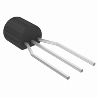
LP2950ACZ-5.0RAG ON Semiconductor, LP2950ACZ-5.0RAG Datasheet - Page 4

LP2950ACZ-5.0RAG
Manufacturer Part Number
LP2950ACZ-5.0RAG
Description
IC REG LDO LP 100MA 5V TO-92
Manufacturer
ON Semiconductor
Datasheet
1.LP2951ACDR2G.pdf
(23 pages)
Specifications of LP2950ACZ-5.0RAG
Regulator Topology
Positive Fixed
Voltage - Output
5V
Voltage - Input
Up to 30V
Voltage - Dropout (typical)
0.35V @ 100mA
Number Of Regulators
1
Current - Output
100mA
Operating Temperature
-40°C ~ 125°C
Mounting Type
Through Hole
Package / Case
TO-92-3 (Standard Body), TO-226
Number Of Outputs
1
Polarity
Positive
Input Voltage Max
30 V
Output Voltage
5 V
Output Type
Fixed
Dropout Voltage (max)
0.08 V at 100 uA
Output Current
100 mA
Line Regulation
0.1 %
Load Regulation
0.1 %
Voltage Regulation Accuracy
0.5 %
Maximum Operating Temperature
+ 125 C
Mounting Style
Through Hole
Minimum Operating Temperature
- 40 C
Reference Voltage
1.26 V
Primary Input Voltage
6V
Output Voltage Fixed
5V
Dropout Voltage Vdo
350mV
No. Of Pins
3
Operating Temperature Range
-40°C To +125°C
Leaded Process Compatible
Yes
Rohs Compliant
Yes
Lead Free Status / RoHS Status
Lead free / RoHS Compliant
Current - Limit (min)
-
Lead Free Status / Rohs Status
Lead free / RoHS Compliant
Other names
LP2950ACZ-5.0RAG
LP2950ACZ-5.0RAGOSTR
LP2950ACZ-5.0RAGOSTR
Available stocks
Company
Part Number
Manufacturer
Quantity
Price
Company:
Part Number:
LP2950ACZ-5.0RAG
Manufacturer:
ON Semiconductor
Quantity:
4 600
Part Number:
LP2950ACZ-5.0RAG
Manufacturer:
ON/安森美
Quantity:
20 000
1. The Junction−to−Ambient Thermal Resistance is determined by PCB copper area per Figure 29.
2. This device series contains ESD protection and exceeds the following tests:
3. Low duty pulse techniques are used during test to maintain junction temperature as close to ambient as possible.
4. V
5. Noise tests on the LP2951 are made with a 0.01 mF capacitor connected across Pins 7 and 1.
*NCV prefix is for automotive and other applications requiring site and change control.
ELECTRICAL CHARACTERISTICS
unless otherwise noted.)
Output Voltage, 5.0 V Versions
Output Voltage, 3.3 V Versions
Output Voltage, 3.0 V Versions
V
V
V
O(nom)
T
V
T
V
T
V
in
in
in
A
A
A
Human Body Model (HBM), 2000 V, Class 2, JESD22 A114−C
Machine Model (MM), 200 V, Class B, JESD22 A115−A
Charged Device Model (CDM), 2000 V, Class IV, JESD22 C101−C
in
in
in
= 6.0 V, I
LP2950C−5.0/LP2951C/NCV2951C*
LP2950AC−5.0/LP2951AC/NCV2951AC*
LP2950C−5.0/LP2951C/NCV2951C*
LP2950AC−5.0/LP2951AC/NCV2951AC*
LP2950C−5.0/LP2951C/NCV2951C*
LP2950AC−5.0/LP2951AC/NCV2951AC*
= 4.3 V, I
LP2950C−3.3/LP2951C−3.3
LP2950AC−3.3/LP2951AC−3.3/NCV2951AC−3.3*
LP2950C−3.3/LP2951C−3.3
LP2950AC−3.3/LP2951AC−3.3/NCV2951AC−3.3*
LP2950C−3.3/LP2951C−3.3
LP2950AC−3.3/LP2951AC−3.3/NCV2951AC−3.3*
= 4.0 V, I
LP2950C−3.0/LP2951C−3.0
LP2950AC−3.0/LP2951AC−3.0
LP2950C−3.0/LP2951C−3.0
LP2950AC−3.0/LP2951AC−3.0
LP2950C−3.0/LP2951C−3.0
LP2950AC−3.0/LP2951AC−3.0
= − 40 to +125°C
= − 40 to +125°C
= − 40 to +125°C
= 6.0 to 30 V, I
= 4.3 to 30 V, I
= 4.0 to 30 V, I
is the part number voltage option.
O
O
O
= 100 mA, T
= 100 mA, T
= 100 mA, T
O
O
O
= 100 mA to 100 mA, T
= 100 mA to 100 mA, T
= 100 mA to 100 mA, T
A
A
A
= 25°C
= 25°C
= 25°C
Characteristic
(V
in
= V
A
A
A
O
= − 40 to +125°C
= − 40 to +125°C
= − 40 to +125°C
+ 1.0 V, I
http://onsemi.com
O
= 100 mA, C
4
O
= 1.0 mF, T
Symbol
A
= 25°C [Note 3],
V
V
V
O
O
O
4.950
4.975
4.900
4.940
4.880
4.925
3.267
3.284
3.234
3.260
3.221
3.254
2.970
2.985
2.940
2.964
2.928
2.958
Min
5.000
5.000
3.300
3.300
3.000
3.000
Typ
−
−
−
−
−
−
−
−
−
−
−
−
5.050
5.025
5.100
5.060
5.120
5.075
3.333
3.317
3.366
3.340
3.379
3.346
3.030
3.015
3.060
3.036
3.072
3.042
Max
Unit
V
V
V


