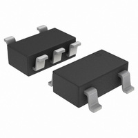
NCP502SN50T1G ON Semiconductor, NCP502SN50T1G Datasheet

NCP502SN50T1G
Specifications of NCP502SN50T1G
NCP502SN50T1GOSTR
Available stocks
Related parts for NCP502SN50T1G
NCP502SN50T1G Summary of contents
Page 1
NCP502, NCP502A 80 mA CMOS Low Iq, Low- Dropout Voltage Regulator The NCP502/A series of fixed output linear regulators are designed for handheld communication equipment and portable battery powered applications which require low quiescent. The NCP502/A series features an ultra−low ...
Page 2
PIN FUNCTION DESCRIPTION Á Á Á Á ...
Page 3
ELECTRICAL CHARACTERISTICS otherwise noted.) Characteristic Output Voltage (T = 25° mA) V out A 1.5 V 1.8 V 2.5 V 2.7 V 2.8 V 2.9 V 3.0 V 3.1 V 3.3 V 3.4 V 3.5 V 3.6 ...
Page 4
V = 3.0 V OUT INPUT VOLTAGE (V) IN Figure 2. Quiescent Current versus Input Voltage ...
Page 5
OUT 2.99 2.985 2.98 2.975 2.97 2.965 2.96 −60 −40 − TEMPERATURE (°C) Figure 8. Output Voltage versus Temperature 1200 1000 800 600 400 200 0 −50 Figure 10. Dropout Voltage ...
Page 6
Load Regulation The change in output voltage for a change in output current at a constant temperature. Dropout Voltage The input/output differential at which the regulator output no longer maintains regulation against further reductions in input voltage. Measured when the ...
Page 7
A typical application circuit for the NCP502/A series is shown in Figure 1, front page. Input Decoupling (C1) A 1.0 mF capacitor either ceramic or tantalum is recommended and should be connected close to the NCP502/A package. Higher values and ...
Page 8
ORDERING INFORMATION Nominal Output Voltage Device NCP502SQ15T1G NCP502SQ15T2G NCP502SQ18T1G NCP502SQ18T2G NCP502SQ25T1G NCP502SQ25T2G NCP502SQ27T1G NCP502SQ27T2G NCP502SQ28T1G NCP502SQ28T2G NCP502SQ29T1G NCP502SQ29T2G NCP502SQ30T1G NCP502SQ30T2G NCP502SQ31T1G NCP502SQ31T2G NCP502SQ33T1G NCP502SQ33T2G NCP502SQ34T1G NCP502SQ34T2G NCP502SQ35T1G NCP502SQ35T2G NCP502SQ36T1G NCP502SQ36T2G NCP502SQ37T1G NCP502SQ37T2G NCP502SQ50T1G NCP502SQ50T2G NCP502ASQ15T1G NCP502ASQ18T1G NCP502ASQ25T1G NCP502ASQ27T1G NCP502ASQ28T1G NCP502ASQ30T1G ...
Page 9
... NCP502SN33T1G NCP502SN34T1G NCP502SN35T1G NCP502SN36T1G NCP502SN37T1G NCP502SN50T1G Additional voltages in 100 mV steps are available upon request by contacting your ON Semiconductor representative. †For information on tape and reel specifications, including part orientation and tape sizes, please refer to our Tape and Reel Packaging Specifications Brochure, BRD8011/D. Marking 2 ...
Page 10
... C H SOLDERING FOOTPRINT* 0.50 0.0197 0.40 0.0157 *For additional information on our Pb−Free strategy and soldering details, please download the ON Semiconductor Soldering and Mounting Techniques Reference Manual, SOLDERRM/D. SQ SUFFIX CASE 419A−02 ISSUE J NOTES: 1. DIMENSIONING AND TOLERANCING PER ANSI Y14.5M, 1982. 2. CONTROLLING DIMENSION: INCH. ...
Page 11
... H T *For additional information on our Pb−Free strategy and soldering details, please download the ON Semiconductor Soldering and Mounting Techniques Reference Manual, SOLDERRM/D. ON Semiconductor and are registered trademarks of Semiconductor Components Industries, LLC (SCILLC). SCILLC reserves the right to make changes without further notice to any products herein. SCILLC makes no warranty, representation or guarantee regarding the suitability of its products for any particular purpose, nor does SCILLC assume any liability arising out of the application or use of any product or circuit, and specifically disclaims any and all liability, including without limitation special, consequential or incidental damages. “ ...


