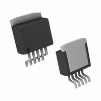
LM2991S/NOPB National Semiconductor, LM2991S/NOPB Datasheet - Page 7

LM2991S/NOPB
Manufacturer Part Number
LM2991S/NOPB
Description
IC REG NEG LDO ADJ V 1A TO-263-5
Manufacturer
National Semiconductor
Datasheet
1.LM2991TNOPB.pdf
(14 pages)
Specifications of LM2991S/NOPB
Regulator Topology
Negative Adjustable
Voltage - Output
-3 ~ -24 V
Voltage - Input
0.3 ~ -26 V
Voltage - Dropout (typical)
0.6V @ 1A
Number Of Regulators
1
Current - Output
1A
Current - Limit (min)
1.5A
Operating Temperature
-40°C ~ 125°C
Mounting Type
Surface Mount
Package / Case
TO-263-5, D²Pak (5 leads + Tab), TO-263BA
Number Of Outputs
1
Polarity
Negative
Input Voltage Max
0.3 V
Output Voltage
- 3 V to - 24 V
Output Type
Adjustable
Dropout Voltage (max)
0.2 V at 100 mA
Output Current
1 A
Line Regulation
0.04 %/V
Load Regulation
0.4 %
Maximum Operating Temperature
+ 125 C
Mounting Style
SMD/SMT
Minimum Operating Temperature
- 40 C
Reference Voltage
- 1.186 V
Lead Free Status / RoHS Status
Lead free / RoHS Compliant
Other names
*LM2991S
*LM2991S/NOPB
LM2991S
*LM2991S/NOPB
LM2991S
Available stocks
Company
Part Number
Manufacturer
Quantity
Price
Application Hints
EXTERNAL CAPACITORS
Like any low-dropout regulator, external capacitors are re-
quired to stabilize the control loop. These capacitors must be
correctly selected for proper performance.
INPUT CAPACITOR
An input capacitor is required if the regulator is located more
than 6 inches from the input power supply filter capacitor (or
if no other input capacitor is present).
A solid Tantalum or ceramic capacitor whose value is at least
1 µF is recommended, but an aluminum electrolytic (
may be used. However, aluminum electrolytic types should
not be used in applications where the ambient temperature
can drop below 0°C because their internal impedance in-
creases significantly at cold temperatures.
OUTPUT CAPACITOR
The output capacitor must meet the ESR limits shown in
ure
mΩ and 10Ω.
A solid Tantalum (value
output capacitor. An aluminum electrolytic (
used if the ESR is in the stable range.
It should be noted that the ESR of a typical aluminum elec-
trolytic will increase by as much as 50X as the temperature is
reduced from 25°C down to −40°C, while a Tantalum will ex-
hibit an ESR increase of about 2X over the same range. For
this and other reasons, aluminum electrolytics should not be
used in applications where low operating temperatures occur.
The lower stable ESR limit of 25 mΩ means that ceramic ca-
pacitors can not be used directly on the output of an LDO. A
ceramic (
resistance is placed in series with it (1Ω recommended). Di-
1, which means it must have an ESR between about 25
FIGURE 1. Output Capacitor ESR Range
≥
2.2 µF) can be used on the output if some external
≥
1 µF) is the best choice for the
≥
10 µF) may be
1126005
≥
10 µF)
Fig-
7
electric types X7R or X5R must be used if the temperature
range of the application varies more than ± 25° from ambient
to assure the amount of capacitance is sufficient.
CERAMIC BYPASS CAPACITORS
Many designers place distributed ceramic capacitors whose
value is in the range of 1000 pF to 0.1 µF at the power input
pins of the IC's across a circuit board. These can cause re-
duced phase margin or oscillations in LDO regulators.
The advent of multi-layer boards with dedicated power and
ground planes has removed the trace inductance that (previ-
ously) provided the necessary "de-coupling" to shield the
output of the LDO from the effects of bypass capacitors.
These capacitors should be avoided if possible, and kept as
far away from the LDO output as is practical.
MINIMUM LOAD
A minimum load current of 500 μA is required for proper op-
eration. The external resistor divider can provide the minimum
load, with the resistor from the adjust pin to ground set to 2.4
kΩ.
SETTING THE OUTPUT VOLTAGE
The output voltage of the LM2991 is set externally by a re-
sistor divider using the following equation:
where V
within the range of −3V to −24V, typically an even greater
range of −2V to −25V. The adjust pin current is about 60 nA,
causing a slight error in the output voltage. However, using
resistors lower than 100 kΩ makes the error due to the adjust
pin current negligible. For example, neglecting the adjust pin
current, and setting R2 to 100 kΩ and V
an output voltage error of only 0.16%.
ON/OFF PIN
The LM2991 regulator can be turned off by applying a TTL or
CMOS level high signal to the ON/OFF pin. The impedance
of the voltage source driving the ON/OFF pin should be low
enough to source the ON/OFF pin input current to meet the
OFF threshold voltage level, 100 µA maximum at 2.4V.
If the ON/OFF function is not needed, the pin should be con-
nected to Ground. The ON/OFF pin should not be left floating,
as this is not a guaranteed operating condition.
See the Adjustable Current Sink Application,
FORCING THE OUTPUT POSITIVE
Due to an internal clamp circuit, the LM2991 can withstand
positive voltages on its output. If the voltage source pulling
the output positive is DC, the current must be limited to 1.5A.
A current over 1.5A fed back into the LM2991 could damage
the device. The LM2991 output can also withstand fast posi-
tive voltage transients up to 26V, without any current limiting
of the source. However, if the transients have a duration of
over 1 ms, the output should be clamped with a Schottky
diode to ground.
REF
V
= −1.21V. The output voltage can be programmed
OUT
= V
REF
x (1 + R
2
/R
1
) − (I
OUT
ADJ
to −5V, results in
x R
Figure 3
2
www.national.com
)


