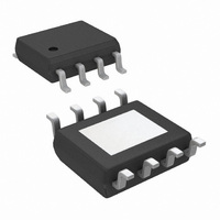
LP38852MR-ADJ/NOPB National Semiconductor, LP38852MR-ADJ/NOPB Datasheet - Page 13

LP38852MR-ADJ/NOPB
Manufacturer Part Number
LP38852MR-ADJ/NOPB
Description
IC REG LDO 1.5A LOW I/O 8-PSOP
Manufacturer
National Semiconductor
Series
PowerWise®r
Datasheet
1.LP38852EVAL.pdf
(18 pages)
Specifications of LP38852MR-ADJ/NOPB
Regulator Topology
Positive Adjustable
Voltage - Output
0.8 ~ 1.8 V
Voltage - Input
0.93 ~ 5.5 V
Voltage - Dropout (typical)
0.13V @ 1.5A
Number Of Regulators
1
Current - Output
1.5A (Max)
Operating Temperature
-40°C ~ 125°C
Mounting Type
Surface Mount
Package / Case
8-PSOP
For Use With
LP38852EVAL - BOARD EVALUATION LP38852
Lead Free Status / RoHS Status
Lead free / RoHS Compliant
Current - Limit (min)
-
Other names
LP38852MR-ADJ
Available stocks
Company
Part Number
Manufacturer
Quantity
Price
Typical C
providing typical Soft-Start times in the range of 70 μs to 7 ms
(5τ). Values less than 1 nF can be used, but the Soft-Start
effect will be minimal. Values larger than 100 nF will provide
soft-start, but may not be fully discharged if V
the UVLVO threshold to less than 500 mV in less than 100
µs.
Figure 2
a typical C
The C
back to the device ground pin. No components, other than
C
adverse effects to V
If the Soft-Start function is not needed the SS pin should be
left open, although some minimal capacitance value is always
recommended.
ENABLE OPERATION
The Enable pin (EN) provides a mechanism to enable, or dis-
able, the regulator output stage. The Enable pin has an
internal pull-up, through a typical 180 kΩ resistor, to V
If the Enable pin is actively driven, pulling the Enable pin
above the V
lator output on, while pulling the Enable pin below the V
threshold will turn the regulator output off. There is approxi-
mately 100 mV of hysteresis built into the Enable threshold
provide noise immunity.
If the Enable function is not needed this pin should be left
open, or connected directly to V
open, stray capacitance on this pin must be minimized, oth-
erwise the output turn-on will be delayed while the stray
capacitance is charged through the internal resistance (r
POWER DISSIPATION AND HEAT-SINKING
Additional copper area for heat-sinking may be required de-
pending on the maximum device dissipation (P
maximum anticipated ambient temperature (T
vice. Under all possible conditions, the junction temperature
must be within the range specified under operating condi-
tions.
The total power dissipation of the device is the sum of three
different points of dissipation in the device.
SS
, should be connected to the SS pin, as there could be
SS
capacitor must be connected to a clean ground path
shows the relationship between the C
SS
FIGURE 2. Typical C
SS
EN
values will be in the range of 1 nF to 100 nF,
value.
threshold of 1.25V (typical) will turn the regu-
OUT
.
SS
BIAS
vs C
. If the Enable pin is left
OUT
Values
BIAS
OUT
A
20213923
) for the de-
D
value and
) and the
falls from
BIAS
EN
.
EN
).
13
The first part is the power that is dissipated in the NMOS pass
element, and can be determined with the formula:
The second part is the power that is dissipated in the bias and
control circuitry, and can be determined with the formula:
where I
of the device that is related to V
The third part is the power that is dissipated in portions of the
output stage circuitry, and can be determined with the formu-
la:
where I
of the device that is related to V
The total power dissipation is then:
The maximum allowable junction temperature rise (ΔT
pends on the maximum anticipated ambient temperature
(T
junction temperature (T
The maximum allowable value for junction to ambient Ther-
mal Resistance, θ
Heat-Sinking The TO-220 Package
The TO-220 package has a θ
rating of 3°C/W. These ratings are for the package only, no
additional heat-sinking, and with no airflow. If the needed
θ
then no additional heat-sinking is required since the package
can safely dissipate the heat and not exceed the operating
T
heat-sinking is needed.
The thermal resistance of a TO-220 package can be reduced
by attaching it to a heat sink or a copper plane on a PC board.
If a copper plane is to be used, the values of θ
as shown in next section for TO-263 package.
The heat-sink to be used in the application should have a
heat-sink to ambient thermal resistance, θ
where θ
junction to the ambient air, θ
the case to the surface of the heart-sink, and θ
resistance from the junction to the surface of the case.
For this equation, θ
The value for θ
tor, etc. θ
JA
J(MAX)
A
) for the application, and the maximum allowable operating
, as calculated above, is greater than or equal to 60°C/W
. If the needed θ
GND(BIAS)
GND(IN)
JA
CH
is the required total thermal resistance from the
P
varies between 1.5°C/W to 2.5°C/W. Consult the
P
D
P
D(PASS)
is the portion of the operating ground current
= P
CH
D(BIAS)
is the portion of the operating ground current
P
JA
depends on method of attachment, insula-
D(PASS)
D(IN)
JC
, can be calculated using the formula:
= (V
= V
is about 3°C/W for a TO-220 package.
= V
JA
J(MAX)
BIAS
+ P
is less than 60°C/W then additional
IN
IN
- V
CH
× I
) .
D(BIAS)
× I
JA
OUT
is the thermal resistance from
GND(IN)
BIAS
IN
GND(BIAS)
rating of 60°C/W and a θ
.
) × I
.
+ P
OUT
D(IN)
HA
:
JC
JA
is the thermal
will be same
www.national.com
J
) de-
(10)
(11)
(12)
(13)
(14)
(8)
(9)
JC


