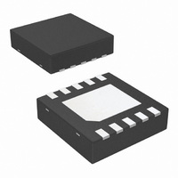
LP3996SD-1525/NOPB National Semiconductor, LP3996SD-1525/NOPB Datasheet - Page 5

LP3996SD-1525/NOPB
Manufacturer Part Number
LP3996SD-1525/NOPB
Description
IC REG LDO 300/150MA DUAL 10-LLP
Manufacturer
National Semiconductor
Datasheet
1.LP3996SD-2828EV.pdf
(18 pages)
Specifications of LP3996SD-1525/NOPB
Regulator Topology
Positive Fixed
Voltage - Output
1.5V, 2.5V
Voltage - Input
2 ~ 6 V
Voltage - Dropout (typical)
-, 0.21V @ 300mA
Number Of Regulators
2
Current - Output
150mA (Min), 300mA (Min)
Operating Temperature
-40°C ~ 85°C
Mounting Type
Surface Mount
Package / Case
10-LLP
For Use With
LP3996SD-3333EV - BOARD EVALUATION LP3996SD-3333LP3996SD-3033EV - BOARD EVALUATION LP3996SD-3033LP3996SD-3030EV - BOARD EVALUATION LP3996SD-3030LP3996SD-2828EV - BOARD EVALUATION LP3996SD-2828
Lead Free Status / RoHS Status
Lead free / RoHS Compliant
Current - Limit (min)
-
Other names
LP3996SD-1525TR
V
ΔV
V
I
I
I
Q
SC
OUT
IN
DO
Absolute Maximum Ratings
(Notes 1, 2)
If Military/Aerospace specified devices are required,
please contact the National Semiconductor Sales Office/
Distributors for availability and specifications.
Electrical Characteristics
Unless otherwise noted, V
V
Typical values and limits appearing in normal type apply for T
temperature range for operation, −40 to +125°C.
Symbol
Input Voltage to GND
V
Voltage to GND
POR to GND
Junction Temperature (T
Lead/Pad Temp. (Note 3)
Storage Temperature
Continuous Power Dissipation
Internally Limited(Note 4)
ESD Rating(Note 5)
Human Body Model
Machine Model
OUT
OUT2
OUT1
. C
, V
IN
OUT2
= 1 µF, I
Input Voltage
Output Voltage Tolerance
Line Regulation Error
Load Regulation Error
Dropout Voltage
(Note 10)
Quiescent Current
Short Circuit Current Limit
Maximum Output Current
EN1 and EN2
OUT
= 1 mA, C
Parameter
J-MAX
EN
= 950mV, V
)
OUT1
-0.3V to (V
= C
IN
OUT2
= V
(Notes 2, 8)
-65°C to 150°C
IN
-0.3V to 6.5V
-0.3V to 6.5V
OUT
= 1.0µF.
(Note 9)
I
V
I
(LDO 1)
I
(LDO 2)
I
(LDO 1)
I
(LDO 2)
LDO 1 ON, LDO 2 ON
I
LDO 1 ON, LDO 2 OFF
I
LDO 1 OFF, LDO 2 ON
I
LDO 1 ON, LDO 2 ON
I
V
LDO 1
LDO 2
LDO 1
LDO 2
+ 0.3V) with
OUT
OUT
OUT
OUT
OUT
OUT1
OUT1
OUT2
OUT1
6.5V (max)
IN
EN1
+ 1.0V, or 2.0V, whichever is higher, where V
= (V
= 1mA
= 1mA to 150mA
= 1mA to 300mA
= 1mA to 150mA
= 1mA to 300mA
= I
= V
= 150mA
= 300mA
= 150mA, I
150°C
235°C
2.0kV
200V
OUT2
OUT(NOM)
EN2
A
= 0mA
= 0.4V
Conditions
= 25°C. Limits appearing in boldface type apply over the full junction
5
OUT2
+ 1.0V) to 6.0V
1.5V < V
V
OUT
Operating Ratings
Thermal Properties
Input Voltage
EN1, EN2, POR Voltage
Junction Temperature
Ambient Temperature T
(Note 6)
Junction To Ambient Thermal
Resistance(Note 7)
θ
= 300mA
JA
≤
LLP-10 Package
1.5V
OUT
≤
3.3V
0.03
Typ
110
210
420
550
0.5
85
26
35
45
45
70
A
Range
OUT
(Notes 1, 2)
is the higher of V
-3.75
-2.75
(Note 1)
Min
-2.5
150
300
-4
2
Limit
0 to (V
+3.75
+2.75
Max
+2.5
155
220
550
100
110
110
170
750
840
0.3
-40°C to 125°C
+4
85
10
6
-40°C to 85°C
2.0V to 6.0V
IN
www.national.com
6.0V (max)
OUT1
+ 0.3V) to
55°C/W
µV/mA
and
Units
%/V
mV
mA
mA
µA
nA
%
V


