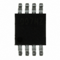
ISL9007IUNZ-T Intersil, ISL9007IUNZ-T Datasheet - Page 6

ISL9007IUNZ-T
Manufacturer Part Number
ISL9007IUNZ-T
Description
IC REG LDO LOW NOISE 3.3V 8-MSOP
Manufacturer
Intersil
Datasheet
1.ISL9007IUFZ-T.pdf
(8 pages)
Specifications of ISL9007IUNZ-T
Regulator Topology
Positive Fixed
Voltage - Output
3.3V
Voltage - Input
Up to 6.5V
Voltage - Dropout (typical)
0.2V @ 400mA
Number Of Regulators
1
Current - Output
400mA (Max)
Current - Limit (min)
470mA
Operating Temperature
-40°C ~ 85°C
Mounting Type
Surface Mount
Package / Case
8-MSOP, Micro8™, 8-uMAX, 8-uSOP,
Lead Free Status / RoHS Status
Lead free / RoHS Compliant
Other names
ISL9007IUNZ-TTR
Pin Descriptions
Typical Application
Block Diagram
SHUTDOWN
VIN (3.0V TO 6.5V)
NUMBER
VIN
VIN
SD
2, 3, 4
PIN
1
5
6
7
8
CONTROL
ON
LOGIC
UVLO
PIN NAME
BANDGAP AND
TEMPERATURE
OFF
GND
VIN
VIN
VO
NC
SD
SENSOR
C
C1
1
, C
2
THERMAL PROTECTION,
: 1µF X5R CERAMIC CAPACITOR
LDO Output:
Connect capacitor of value 1µF to 10µF to
GND (1µF recommended)
No Connection
GND is the connection to system ground.
Connect to PCB Ground plane.
LDO Shutdown. When this signal goes
high, the LDO is turned off.
Supply Voltage/LDO Input:
Connect a 1µF capacitor to GND.
Supply Voltage/LDO Input:
Connect a 1µF capacitor to GND.
SHORT CIRCUIT,
8
7
6
SOFT-START
+
-
6
VIN
VIN
SD
ISL9007
DESCRIPTION
GND
VO
1
5
C2
VOUT
VO
GND
ISL9007
Functional Description
The ISL9007 contains all circuitry required to implement a
high performance LDO. High performance is achieved
through a circuit that delivers fast transient response to
varying load conditions. In a quiescent condition, the
ISL9007 adjusts its biasing to achieve the lowest standby
current consumption.
The device also integrates current limit protection, smart
thermal shutdown protection, and soft-start. Smart thermal
shutdown protects the device against overheating. Soft-start
minimize start-up input current surges without causing
excessive device turn-on time.
Power Control
The ISL9007 has a shutdown pin (SD) to control power to
the LDO output. When SD is high, the device is in shutdown
mode. In this condition, all on-chip circuits are off, and the
device draws minimum current, typically less than 0.1µA.
When the SD pin goes low, the device first polls the output of
the UVLO detector to ensure that VIN voltage is at least 2.1V
(typical). Once verified, the device initiates a start-up
sequence. During the start-up sequence, trim settings are
first read and latched. Then, sequentially, the bandgap,
reference voltage and current generation circuitry turn-on.
Once the references are stable, the LDO powers up.
During operation, whenever the VIN voltage drops below
about 1.84V, the ISL9007 immediately disables both LDO
outputs. When VIN rises back above 2.1V (assuming the SD
pin is low), the device re-initiates its start-up sequence and
LDO operation will resume automatically.
Reference Generation
The reference generation circuitry includes a trimmed
bandgap, a trimmed voltage reference divider, a trimmed
current reference generator, and an RC noise filter.
The bandgap generates a zero temperature coefficient (TC)
voltage for the regulator reference and other voltage
references required for current generation and
over-temperature detection.
A current generator provides references required for
adaptive biasing as well as references for LDO output
current limit and thermal shutdown determination.
LDO Regulation and Programmable Output Divider
The LDO Regulator is implemented with a high-gain
operational amplifier driving a PMOS pass transistor. The
design of the ISL9000 provides a regulator that has low
quiescent current, fast transient response, and overall
stability across all operating and load current conditions.
LDO stability is guaranteed for a 1µF to 10µF output
capacitor that has a tolerance better than 20% and ESR less
than 200mΩ. The design is performance-optimized for a 1µF
capacitor. Unless limited by the application, use of an output
October 30, 2008
FN9218.2


