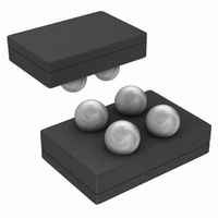
LP3991TLX-2.8/NOPB National Semiconductor, LP3991TLX-2.8/NOPB Datasheet - Page 10

LP3991TLX-2.8/NOPB
Manufacturer Part Number
LP3991TLX-2.8/NOPB
Description
IC VREG 300MA 2.8V 4-USMD
Manufacturer
National Semiconductor
Series
PowerWise®r
Datasheet
1.LP3991TL-1.2EV.pdf
(12 pages)
Specifications of LP3991TLX-2.8/NOPB
Regulator Topology
Positive Fixed
Voltage - Output
2.8V
Voltage - Input
Up to 4V
Voltage - Dropout (typical)
0.075V @ 300mA
Number Of Regulators
1
Current - Output
300mA (Min)
Operating Temperature
-40°C ~ 85°C
Mounting Type
Surface Mount
Package / Case
4-MicroSMD
For Use With
LP3991TL-1.8EV - BOARD EVALUATION LP3991TL-1.8
Lead Free Status / RoHS Status
Lead free / RoHS Compliant
Current - Limit (min)
-
Other names
LP3991TLX-2.8
Available stocks
Company
Part Number
Manufacturer
Quantity
Price
Company:
Part Number:
LP3991TLX-2.8/NOPB
Manufacturer:
Texas Instruments
Quantity:
10 000
www.national.com
1µF to 4.7µF range. Another important consideration is that
tantalum capacitors have higher ESR values than equivalent
size ceramics. This means that while it may be possible to find
a tantalum capacitor with an ESR value within the stable
range, it would have to be larger in capacitance (which means
bigger and more costly) than a ceramic capacitor with the
same ESR value. It should also be noted that the ESR of a
typical tantalum will increase about 2:1 as the temperature
goes from 25°C down to -40°C, so some guard band must be
allowed.
ENABLE CONTROL
The LP3991 features an active high Enable pin, V
turns the device on when pulled high. When not enabled the
regulator output is off and the device typically consumes 2nA.
If the application does not require the Enable switching fea-
ture, the V
output permanently on.
To ensure proper operation, the signal source used to drive
the V
specified turn-on/off voltage thresholds listed in the Electrical
Characteristics section under V
POST-BUCK REGULATOR
Linear Post-Regulation can be an effective way to reduce rip-
ple and switching noise from DC/DC convertors while still
maintaining a reasonably high overall efficiency.
The LP3991 is particularly suitable for this role due to its low
input voltage requirements. In addition, there is often no need
for a separate input capacitor for the LP3991 as it can share
the output cap of the DC/DC convertor.
Care of PCB layouts involving switching regulators is
paramount. In particular, the ground paths for the LDO should
be routed separately from the switcher ground and star con-
nected close to the battery. Routing of the switch pin of the
DC/DC convertor must be kept short to minimize radiated
EMI. A low pass filter such as a ferrite bead or common mode
choke on the battery input leads can further reduce radiated
EMI.
Figure 2
DC/DC buck regulator with a nominal output of 1.8V and a
1.5V LP3991. The overall efficiency will be greater than 70%
over the full Li-Ion battery voltage range. Maximum efficiency
is achieved by minimizing the difference between V
V
down to an input voltage of 1.65V, so, in this case, a 1.8V
buck with 5% tolerance is adequate for all conditions of tem-
perature and load.
OUT
of the LP3991. The LP3991-1.5 will remain in regulation
EN
input must be able to swing above and below the
shows a typical example using an LM3673, 350mA
EN
pin should be tied to V
IL
and V
IN
FIGURE 2. LP3991 Used as a Post DC/DC regulator
to keep the regulator
IH
.
EN
, which
IN
and
10
micro SMD MOUNTING
The micro SMD package requires specific mounting tech-
niques which are detailed in the National Semiconductor
Application Note (AN-1112). Referring to the section Surface
Mount Technology (SMT) Assenbly Considerations, it should
be noted that the pad style which must be used with the 4 pin
package is NSMD (non-solder mask defined) type.
For best results during assembly, alignment ordinals on the
PCB may be used to facilitate placement of the micro SMD
device.
micro SMD LIGHT SENSITIVITY
Exposing the micro SMD device to direct sunlight may cause
mis-operation of the device. Light sources such as halogen
lamps can affect the electrical performance if brought near to
the device.
The wavelengths which have most detrimental effect are reds
and infra-reds, which means that fluorescent lighting, used
inside most buildings will have little effect on performance.
MAXIMUM SUPPLY VOLTAGE AND THERMAL
CONSIDERATIONS
Maximum recommended input voltage is 3.6V. The device
may be operated at 4.0V V
board design in regard to thermal dissipation. As a guide
please refer to the following table for ambient temperature at
2 input voltages and 2 load currents for the example board
types.
160ºC/W
88ºC/W
θ
JA
3.6V 2.8V
4.0V 2.8V
3.6V 2.8V
4.0V 2.8V
V
IN
V
OUT
160mA
250mA
160mA
250mA
160mA
250mA
160mA
250mA
IN
I
OUT
if proper care is given to the
0.130W
0.200W
0.190W
0.300W
0.130W
0.200W
0.190W
0.300W
P
D
20110036
Ambient
Temp.
113ºC
107ºC
108ºC
104ºC
98ºC
93ºC
94ºC
77ºC


