XC6221B1827R-G Torex Semiconductor Ltd, XC6221B1827R-G Datasheet
XC6221B1827R-G
Specifications of XC6221B1827R-G


Related parts for XC6221B1827R-G


XC6221B1827R-G Summary of contents
Page 1
XC6221 Series ■GENERAL DESCRIPTION The XC6221 series is a high accuracy, low noise, high speed, low dropout CMOS regulator with high ripple rejection. The series includes a reference voltage source, an error amplifier, a current limiter, and a phase compensation ...
Page 2
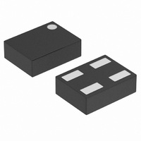
XC6221 Series ■PIN CONFIGURATION OUT IN USP-4 (BOTTOM VIEW *It is recommended that the heat dissipation pad of the USP package is ...
Page 3
FUNCTION ASSIGNMENT XC6221A/B (CE no pull-down resistor) CE LEVEL HIGH LOW OPEN XC6221C/D (CE pull-down resistor) CE LEVEL HIGH LOW OPEN ■PRODUCT CLASSIFICATION ●Ordering Information (*1) XC6221 ①②③④⑤⑥-⑦ DESIGNATOR ITEM Type of Regulator ① Output Voltage ②③ ④ Output ...
Page 4
XC6221 Series ■BLOCK DIAGRAMS ON/OFF CE Control - Error Current Amp CE CE/ Limit + each circuit Voltage Reference ●XC6221A Series XC6221Aシリーズ ON/OFF CE Control R Pull -down - Error Current Amp Limit CE CE/ + each circuit Voltage Reference ...
Page 5
CHARACTERISTICS ●XC6221A/B/C/D series PARAMETER SYMBOL Output Voltage V OUT( (Standard) Output Voltage V OUT( (High Accuracy) Output Current I OUTMAX Load Regulation V (*5) Dropout Voltage Vdif Supply Current I DD Standby Current I STB ...
Page 6
XC6221 Series ■OUTPUT VOLTAGE CHART OUTPUT VOLTAGE NOMINAL (Standard) OUTPUT V VOLTAGE OUT(E) (V) (V) MIN. MAX. 0.80 0.7700 0.8300 0.85 0.8200 0.8800 0.90 0.8700 0.9300 0.95 0.9200 0.9800 1.00 0.9700 1.0300 1.05 1.0200 1.0800 1.10 1.0700 1.1300 1.15 1.1200 ...
Page 7
VOLTAGE CHART (Continued) OUTPUT VOLTAGE NOMINAL (Standard) OUTPUT V VOLTAGE OUT(E) (V) (V) MIN. MAX. 3.00 2.9400 3.0600 3.05 2.8990 3.1100 3.10 3.0380 3.1620 3.15 3.0870 3.2130 3.20 3.1360 3.2640 3.25 3.1850 3.3150 3.30 3.2340 3.3660 3.35 3.2830 3.4170 ...
Page 8
XC6221 Series ■OPERATIONAL EXPLANATION <Output Voltage Control> The voltage divided by resistors R1 & compared with the internal reference voltage by the error amplifier. The P-channel MOSFET connected to the V V pin is controlled & stabilized by ...
Page 9
EXPLANATION (Continued) <Current Limiter, Short-Circuit Protection> The XC6221 series’ fold-back circuit operates as an output current limiter and a short protection circuit for the output pin. When the load current reaches the current limit level, the fixed current limiter ...
Page 10
XC6221 Series ■TEST CIRCUITS Circuit 1: Output Voltage, Output Current, Dropout Voltage, Input/Operating Voltage, Line Regulation, Load Regulation, Current Limit, Short Current, CL Discharge Resistance Circuit 2: Supply Current, Stand-by Current Circuit 3: Ripple Rejection Rate 10/28 ...
Page 11
CIRCUITS (Continued) Circuit 4: CE “H” “L” Level Voltage, CE “H” “L” Level Current C IN (ceramic OUT (ceramic) V XC6221 Series V 11/28 ...
Page 12
XC6221 Series ■TYPICAL PERFORMANCE CHARACTERISTICS (1) Output Voltage vs. Output Current XC6221x182 Ta=25℃ =1.0μF (ceramic 2.4 1.8 1.2 0 100 200 Output Current: I XC6221x302 Ta=25℃ ...
Page 13
PERFORMANCE CHARACTERISTICS (Continued) (2) Output Voltage vs. Input Voltage (Continued) XC6221x302 Ta=25℃ =1.0μF (ceramic 3.2 3.1 3 2.9 2.8 2.7 2.6 2.5 2 2.5 3 Input Voltage (3) ...
Page 14
XC6221 Series ■TYPICAL PERFORMANCE CHARACTERISTICS (Continued) (5) Supply Current vs. Input Voltage XC6221x182 =1.0μF (ceramic Ta=85℃ 60 Ta=25℃ Ta=-40℃ Input ...
Page 15
PERFORMANCE CHARACTERISTICS (Continued) (8) Line Transient Response XC6221x182 Tr=Tf=5μ =1mA , Ta=25℃ =1.0μF(ceramic) OUT L 5 Input Voltage Output Voltage Time: (20μs/div) XC6221x182 V =V ...
Page 16
XC6221 Series ■TYPICAL PERFORMANCE CHARACTERISTICS (Continued) (9) Input Rise Characteristics XC6221x182xx Tr=5μ =1mA , Ta=25℃ =1.0μF (ceramic) OUT L 4 Input Voltage Output Voltage - Time: ...
Page 17
PERFORMANCE CHARACTERISTICS (Continued) (10) CE Rise Characteristics XC6221x182 V =2.8V, Tr=5μ =1mA ,Ta=25℃ =1.0μF (ceramic) OUT Input Voltage Output Voltage - Time: (40μs/div) XC6221x182 ...
Page 18
XC6221 Series ■TYPICAL PERFORMANCE CHARACTERISTICS (Continued) (11) Ripple Rejection Rate XC6221x182 V =V =2.8V +0. P-PAC I =30mA , Ta=25℃ =1.0μF (ceramic) OUT 0.01 0.1 ...
Page 19
INFORMATION ●USP-4 (unit : mm) ●SSOT-24 (unit : mm) ●SOT-25 (unit : mm) * Soldering f illet surf ace is not f ormed because the sides of the pins are plated. ●USPN-4 (unit : mm) XC6221 Series 19/28 ...
Page 20
XC6221 Series ■PACKAGING INFORMATION (Continued) ●USP-4 Reference Pattern Layout (unit : mm) ●USPN-4 Reference Pattern Layout (unit : mm) 20/28 ●USP-4 Reference Metal Mask Design (unit : mm) ●USPN-4 Reference Metal Mask Design (unit : mm) ...
Page 21
INFORMATION (Continued) ● USP-4 Power Dissipation Power dissipation data for the USP-4 is shown in this page. The value of power dissipation varies with the mount board conditions. Please use this data as one of reference data taken in ...
Page 22
XC6221 Series ■PACKAGING INFORMATION (Continued) ● SOT-25 Power Dissipation Power dissipation data for the SOT-25 is shown in this page. The value of power dissipation varies with the mount board conditions. Please use this data as one of reference data ...
Page 23
INFORMATION (Continued) ● SSOT-24 Power Dissipation Power dissipation data for the SSOT-24 is shown in this page. The value of power dissipation varies with the mount board conditions. Please use this data as one of reference data taken in ...
Page 24
XC6221 Series ■PACKAGING INFORMATION (Continued) ● USPN-4 Power Dissipation Power dissipation data for the USPN-4 is shown in this page. The value of power dissipation varies with the mount board conditions. Please use this data as one of reference data ...
Page 25
RULE ●SOT-25 / USP ① ② ③ ④ ⑤ SOT-25 USP-4 (TOP VIEW) (TOP VIEW) ② represents type of regulator OUTPUT VOLTAGE 0.1V INCREMENTS V =0.80~3.00V V =3.10~5.00V OUT OUT V A ...
Page 26
XC6221 Series ■MARKING RULE (Continued) ●SSOT-24(Without bar) / USPN USPN-4 SSOT-24 (TOP VIEW) (TOP VIEW) ① represents type of regulator and output voltage range. TYPE OF MARK REGULATOR ...
Page 27
RULE (Continued) ●SSOT-24(With bar) / USPN SSOT-24 USPN-4 (TOP VIEW) (TOP VIEW) ① represents type of regulator and output voltage range. OUTPUT TYPE OF MARK VOLTAGE REGULATOR RANGE( 0.80~3. ...
Page 28
... Should you wish to use the products under conditions exceeding the specifications, please consult us or our representatives assume no responsibility for damage or loss due to abnormal use. 7. All rights reserved. No part of this datasheet may be copied or reproduced without the prior permission of TOREX SEMICONDUCTOR LTD. 28/28 ...