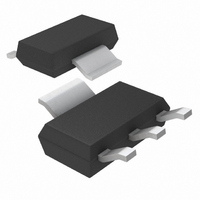
LT1963EST-1.5#PBF Linear Technology, LT1963EST-1.5#PBF Datasheet - Page 6

LT1963EST-1.5#PBF
Manufacturer Part Number
LT1963EST-1.5#PBF
Description
IC REG LDO 1.5V 1.5A LN SOT223-3
Manufacturer
Linear Technology
Specifications of LT1963EST-1.5#PBF
Regulator Topology
Positive Fixed
Voltage - Output
1.5V
Voltage - Input
2.1 ~ 20 V
Voltage - Dropout (typical)
0.34V @ 1.5A
Number Of Regulators
1
Current - Output
1.5A
Current - Limit (min)
1.6A
Operating Temperature
-40°C ~ 125°C
Mounting Type
Surface Mount
Package / Case
SOT-223 (3 leads + Tab), SC-73, TO-261
Primary Input Voltage
2.5V
Output Voltage Fixed
1.5V
Dropout Voltage Vdo
340mV
No. Of Pins
3
Output Current
1.5A
Voltage Regulator Case Style
SOT-223
Operating Temperature Range
-40°C To
Rohs Compliant
Yes
Lead Free Status / RoHS Status
Lead free / RoHS Compliant
Available stocks
Company
Part Number
Manufacturer
Quantity
Price
LT1963A Series
ELECTRICAL CHARACTERISTICS
temperature range, otherwise specifi cations are at T
PARAMETER
Ripple Rejection
Current Limit
Input Reverse Leakage Current (Note 13)
Reverse Output Current (Note 11)
Note 1: Stresses beyond those listed under Absolute Maximum Ratings
may cause permanent damage to the device. Exposure to any Absolute
Maximum Rating condition for extended periods may affect device
reliability and lifetime.
Note 2: Absolute maximum input to output differential voltage can not
be achieved with all combinations of rated IN pin and OUT pin voltages.
With the IN pin at 20V, the OUT pin may not be pulled below 0V. The total
measured voltage from IN to OUT can not exceed ± 20V.
Note 3: The LT1963A regulators are tested and specifi ed under pulse load
conditions such that T
Performance at –40°C and 125°C is assured by design, characterization and
correlation with statistical process controls. The LT1963AI is guaranteed
over the full –40°C to 125°C operating junction temperature range. The
LT1963AMP is 100% tested and guaranteed over the –55°C to 125°C
operating junction temperature range.
Note 4: The LT1963A (adjustable version) is tested and specifi ed for these
conditions with the ADJ pin connected to the OUT pin.
Note 5: Operating conditions are limited by maximum junction
temperature. The regulated output voltage specifi cation will not apply
for all possible combinations of input voltage and output current. When
operating at maximum input voltage, the output current range must be
limited. When operating at maximum output current, the input voltage
range must be limited.
6
J
≈ T
A
. The LT1963AE is 100% tested at T
CONDITIONS
V
f
V
V
Q, T, S8 Packages
ST Package
LT1963A-1.5
LT1963A-1.8
LT1963A-2.5
LT1963A-3.3
LT1963A (Note 4)
RIPPLE
IN
IN
IN
– V
= 7V, V
= V
OUT
OUT(NOMINAL)
= 120Hz, I
OUT
= 1.5V (Avg), V
= 0V
A
LOAD
A
= 25°C. (Note 3)
= 25°C.
+ 1V, ΔV
V
V
V
V
V
V
V
IN
IN
OUT
OUT
OUT
OUT
OUT
= 0.75A
The
= –20V, V
= –20V, V
RIPPLE
= 1.5V, V
= 1.8V, V
= 2.5V, V
= 3.3V, V
= 1.21V, V
l
OUT
denotes specifi cations which apply over the full operating
= 0.5V
= – 0.1V
OUT
OUT
IN
IN
IN
IN
Note 6: To satisfy requirements for minimum input voltage, the LT1963A
(adjustable version) is tested and specifi ed for these conditions with an
external resistor divider (two 4.12k resistors) for an output voltage of 2.4V.
The external resistor divider will add a 300μA DC load on the output.
Note 7: Dropout voltage is the minimum input to output voltage differential
needed to maintain regulation at a specifi ed output current. In dropout, the
output voltage will be equal to: V
Note 8: GND pin current is tested with V
current source load. The GND pin current will decrease at higher input
voltages.
Note 9: ADJ pin bias current fl ows into the ADJ pin.
Note 10: SHDN pin current fl ows into the SHDN pin.
Note 11: Reverse output current is tested with the IN pin grounded and the
OUT pin forced to the rated output voltage. This current fl ows into the OUT
pin and out the GND pin.
Note 12: For the LT1963A, LT1963A-1.5 and LT1963A-1.8 dropout voltage
will be limited by the minimum input voltage specifi cation under some
output voltage/load conditions.
Note 13: For the ST package, the input reverse leakage current increases
due to the additional reverse leakage current for the SHDN pin, which is
tied internally to the IN pin.
IN
< 1.5V
< 1.8V
< 2.5V
< 3.3V
= 0
= 0
P-P
< 1.21V
,
●
●
●
IN
– V
MIN
1.6
55
DROPOUT
IN
= V
OUT(NOMINAL)
.
TYP
600
600
600
600
300
63
2
MAX
1200
1200
1200
1200
600
1
2
+ 1V and a
UNITS
1963afd
mA
mA
dB
μA
μA
μA
μA
μA
A
A


