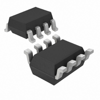
LT3009ESC8-5.0#TRMPBF Linear Technology, LT3009ESC8-5.0#TRMPBF Datasheet - Page 11

LT3009ESC8-5.0#TRMPBF
Manufacturer Part Number
LT3009ESC8-5.0#TRMPBF
Description
IC REG LDO 5V 20MA SC70-8
Manufacturer
Linear Technology
Datasheet
1.LT3009EDCTRMPBF.pdf
(20 pages)
Specifications of LT3009ESC8-5.0#TRMPBF
Regulator Topology
Positive Fixed
Voltage - Output
5V
Voltage - Input
Up to 20V
Voltage - Dropout (typical)
0.28V @ 20mA
Number Of Regulators
1
Current - Output
20mA
Current - Limit (min)
22mA
Operating Temperature
-40°C ~ 125°C
Mounting Type
Surface Mount
Package / Case
SC-70-8
Lead Free Status / RoHS Status
Lead free / RoHS Compliant
PIN FUNCTIONS
SHDN (Pin 1/Pin 5): Shutdown. Pulling the SHDN pin
low puts the LT3009 into a low power state and turns the
output off. If unused, tie the SHDN pin to V
does not function if the SHDN pin is not connected. The
SHDN pin cannot be driven below GND unless tied to the
IN pin. If the SHDN pin is driven below GND while IN is
powered, the output will turn on. SHDN pin logic cannot
be referenced to a negative rail.
GND (Pins 2, 3, 4/Pin 6): Ground. Connect the bottom
of the resistor divider that sets output voltage directly to
GND for the best regulation.
IN (Pin 5/Pin 4): Input. The IN pin supplies power to the
device. The LT3009 requires a bypass capacitor at IN if
the device is more than six inches away from the main
input fi lter capacitor. In general, the output impedance
of a battery rises with frequency, so it is advisable to
include a bypass capacitor in battery-powered circuits. A
bypass capacitor in the range of 0.1μF to 10μF will suf-
fi ce. The LT3009 withstands reverse voltages on the IN
pin with respect to ground and the OUT pin. In the case
of a reversed input, which occurs with a battery plugged
in backwards, the LT3009 acts as if a large resistor is in
series with its input. Limited reverse current fl ows into
the LT3009 and no reverse voltage appears at the load.
The device protects both itself and the load.
(SC70/DFN)
IN
. The LT3009
OUT (Pin 6/Pins 2, 3): Output. This pin supplies power to
the load. Use a minimum output capacitor of 1μF to prevent
oscillations. Large load transient applications require larger
output capacitors to limit peak voltage transients. See the
Applications Information section for more information on
output capacitance and reverse output characteristics.
ADJ (Pin 7/Pin 1): Adjust. This pin is the error amplifi er’s
inverting terminal. Its 300pA typical input bias current
fl ows out of the pin (see curve of ADJ Pin Bias Current vs
Temperature in the Typical Performance Characteristics
section). The ADJ pin voltage is 600mV referenced to GND
and the output voltage range is 600mV to 19.5V. This pin
is not connected in the fi xed output voltage versions.
NC (Pins 7, 8/Pin 1): No Connect. For the adjustable voltage
version, Pin 8 is an NC pin in the SC70 package. For the
fi xed voltage versions, Pin 7 and Pin 8 are NC pins in the
SC70 package, and Pin 1 is an NC pin in the DFN package.
NC pins are not tied to any internal circuitry. They may be
fl oated, tied to V
Exposed Pad (Pin 7, DFN Package Only): Ground. The
Exposed Pad (backside) of the DFN package is an electri-
cal connection to GND. To ensure optimum performance,
solder Pin 7 to the PCB and tie directly to Pin 6.
IN
or tied to GND.
LT3009 Series
11
3009fc


