TC1301A-SFCVUATR Microchip Technology, TC1301A-SFCVUATR Datasheet - Page 14

TC1301A-SFCVUATR
Manufacturer Part Number
TC1301A-SFCVUATR
Description
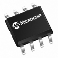
IC REG LDO DUAL 300/150MA 8MSOP
Manufacturer
Microchip Technology
Datasheet
1.TC1301A-ADAVUA.pdf
(28 pages)
Specifications of TC1301A-SFCVUATR
Regulator Topology
Positive Fixed
Voltage - Output
1.5V, 2.8V, 2.32V (Reset)
Voltage - Input
2.7 ~ 6 V
Voltage - Dropout (typical)
-, 0.15V @ 150mA
Number Of Regulators
2
Current - Output
300mA (Min), 150mA (Min)
Operating Temperature
-40°C ~ 125°C
Mounting Type
Surface Mount
Package / Case
8-MSOP, Micro8™, 8-uMAX, 8-uSOP,
Lead Free Status / RoHS Status
Lead free / RoHS Compliant
Current - Limit (min)
-
TC1301A/B
5.0
5.1
The TC1301A/B is a combination device consisting of
one 300 mA LDO regulator with a fixed output voltage,
V
fixed output voltage, V
microcontroller voltage monitor/RESET (2.2V to 3.2V).
For the TC1301A, the 300 mA output (V
present, independent of the level of SHDN2. The
150 mA output (V
controlling the level of SHDN2.
For the TC1301B, V
independent shutdown input pins (SHDN1 and
SHDN2) to control their respective outputs. In the case
of the TC1301B, the voltage detect input of the
microcontroller RESET function is internally connected
to the V
5.2
LDO output #1 is rated for 300 mA of output current.
The typical dropout voltage for V
300 mA. A 1 µF (minimum) output capacitor is needed
for stability and should be located as close to the V
pin and ground as possible.
5.3
LDO output #2 is rated for 150 mA of output current.
The typical dropout voltage for V
(minimum) capacitor is needed for stability and should
be located as close to the V
possible.
5.4
The RESET output is used to detect whether the level
on the input of V
above or below a preset threshold. If the voltage
detected is below the preset threshold, the RESET
output is capable of sinking 1.2 mA (V
maximum). Once the voltage being monitored is above
the preset threshold, the RESET output pin will
transition from a logic-low to a logic-high after a 300 ms
delay. The RESET output is a push-pull configuration
and will actively pull the RESET output up to V
when not in RESET.
5.5
Low input source impedance is necessary for the two
LDO outputs to operate properly. When operating from
batteries or in applications with long lead length
(> 10 inches) between the input source and the LDO,
some input capacitance is recommended. A minimum
of 1.0 µF to 4.7 µF is recommended for most applica-
tions. When using large capacitors on the LDO outputs,
larger capacitance is recommended on the LDO input.
The capacitor should be placed as close to the input of
DS21798C-page 14
OUT1
(1.5V – 3.3V), one 150 mA LDO regulator with a
OUT1
DETAILED DESCRIPTION
Device Overview
LDO Output #1
LDO Output #2
RESET Output
Input Capacitor
output of the device.
DET
OUT2
(TC1301A) or V
OUT1
) can be turned on/off by
OUT2
and V
OUT2
(1.5V – 3.3V), and a
OUT2
OUT1
pin and ground as
OUT1
OUT2
= 150 mV. A 1 µF
OUT1
RESET
= 104 mV @
(TC1301B) is
each have
) is always
< 0.2V
OUT1
DET
the LDO as is practical. Larger input capacitors will help
reduce the input impedance and further reduce any
high-frequency noise on the input and output of the
LDO.
5.6
A minimum output capacitance of 1 µF for each of the
TC1301A/B LDO outputs is necessary for stability.
Ceramic capacitors are recommended because of their
size, cost and environmental robustness qualities.
Electrolytic (Tantalum or Aluminum) capacitors can be
used on the LDO outputs as well. The Equivalent
Series Resistance (ESR) requirements on the
electrolytic output capacitors are between 0 and 2
ohms. The output capacitor should be located as close
to the LDO output as is practical. Ceramic materials,
X7R and X5R, have low temperature coefficients and
are well within the acceptable ESR range required. A
typical 1 uF X5R 0805 capacitor has an ESR of 50 milli-
ohms. Larger LDO output capacitors can be used with
the TC1301A/B to improve dynamic performance and
power supply ripple rejection performance. A maximum
of 10 µF is recommended. Aluminum electrolytic
capacitors are not recommended for low temperature
applications of < -25°C.
5.7
The bypass pin is connected to the internal LDO
reference. By adding capacitance to this pin, the LDO
ripple rejection, input voltage transient response and
output noise performance are all increased. A typical
bypass capacitor between 470 pF to 10 nF is
recommended. Larger bypass capacitors can be used,
but results in a longer time-period for the LDO outputs
to reach their rated output voltage when started from
SHDN or V
5.8
For the optimal noise and PSRR performance, the
GND pin of the TC1301A/B should be tied to a quiet
circuit ground. For applications that have switching or
noisy inputs, tie the GND pin to the return of the output
capacitor. Ground planes help lower inductance and
voltage spikes caused by fast transient load currents
and are recommended for applications that are
subjected to fast load transients.
5.9
The TC1301A SHDN2 pin is used to turn V
and OFF. A logic-high level on SHDN2 will enable the
V
disable the V
not affected by SHDN2 and will be enabled as long as
the input voltage is present.
The TC1301B SHDN1 and SHDN2 pins are used to
turn V
independent of each other.
OUT2
OUT1
output, while a logic-low on the SHDN2 pin will
Output Capacitor
Bypass Input
GND
SHDN1/SHDN2 Operation
IN
and V
.
OUT2
output. For the TC1301A, V
OUT2
© 2008 Microchip Technology Inc.
ON and OFF. They operate
OUT2
OUT1
ON
is


