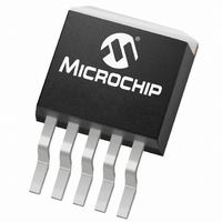
TC1263-2.8VETTR Microchip Technology, TC1263-2.8VETTR Datasheet - Page 7

TC1263-2.8VETTR
Manufacturer Part Number
TC1263-2.8VETTR
Description
IC CMOS LDO 2.8V 500MA DDPAK-5
Manufacturer
Microchip Technology
Datasheet
1.TC1263-3.0VOA.pdf
(18 pages)
Specifications of TC1263-2.8VETTR
Regulator Topology
Positive Fixed
Voltage - Output
2.8V
Voltage - Input
Up to 6V
Voltage - Dropout (typical)
0.35V @ 500mA
Number Of Regulators
1
Current - Output
500mA (Min)
Operating Temperature
-40°C ~ 125°C
Mounting Type
Surface Mount
Package / Case
TO-263-5, D²Pak (5 leads + Tab), TO-263BA
Number Of Outputs
1
Polarity
Positive
Input Voltage Max
6 V
Output Voltage
2.8 V
Output Type
Fixed
Dropout Voltage (max)
650 mV
Output Current
500 mA
Line Regulation
0.05 %
Load Regulation
0.002 % / mA
Voltage Regulation Accuracy
0.5 %
Maximum Operating Temperature
+ 125 C
Mounting Style
SMD/SMT
Minimum Operating Temperature
- 40 C
Lead Free Status / RoHS Status
Lead free / RoHS Compliant
Current - Limit (min)
-
Lead Free Status / Rohs Status
Details
Other names
TC12632.8VETTR
4.0
The TC1263 is a precision, fixed-output LDO. Unlike
bipolar regulators, the TC1263’s supply current does
not increase with load current. In addition, V
remains stable and within regulation over the entire
0 mA to I
consideration in RTC and CMOS RAM battery back-up
applications).
Figure 4-1 shows a typical application circuit.
FIGURE 4-1:
4.1
A 1 µF (min.) capacitor from V
required. The output capacitor should have an Effective
Series Eesistance (ESR) greater than 0.1
than 5 . A 1 µF capacitor should be connected from
V
between the regulator and the AC filter capacitor or a
battery is used as the power source. Aluminum
electrolytic or tantalum capacitor types can be used.
Since many aluminum electrolytic capacitors freeze at
approximately
recommended for applications operating below -25°C.
When operating from sources other than batteries,
supply-noise rejection and transient response can be
improved by increasing the value of the input and
output capacitors, and by employing passive filtering
techniques.
© 2005 Microchip Technology Inc.
Shutdown Control
(to CMOS Logic or Tie
to V
IN
IN
to GND if there is either more than 10 inches of wire
, if unused)
+
DETAILED DESCRIPTION
Battery
Output Capacitor
LOADMAX
+
1 µF
C
1
Processor RESET Signal
if ERROR is used as a
-30°C,
C
GND
3
load current range (an important
SHDN
V
Required Only
IN
(See Text)
Typical Application Circuit.
TC1263
ERROR
solid
V
OUT
OUT
tantalums
+
V
1 µF
C
+
+
2
0.2 µF
C
to ground is
R
1 M
3
1
V
and less
OUT
BATTLOW
or RESET
OUT
are
4.2
ERROR is driven low whenever V
regulation by more than – 5% (typ.). This condition may
be caused by low input voltage, output current limiting
or thermal limiting. The ERROR threshold is 5% below
rated V
voltage value (e.g., ERROR = V
5.0V regulator and 2.85V (typ.) for a 3.0V regulator).
ERROR output operation is shown in Figure 4-2.
Note that ERROR is active when V
V
As shown in Figure 4-1, ERROR can be used as a
battery-low flag or as a processor RESET signal (with
the addition of timing capacitor C
chosen to maintain ERROR below V
RESET input for at least 200 ms to allow time for the
system to stabilize. Pull-up resistor R
V
FIGURE 4-2:
ERROR
TH
OUT
V
V
V
V
OUT
, and inactive when V
OH
OL
TH
, V
IN
OUT
ERROR Output
or any other voltage less than (V
, regardless of the programmed output
ERROR Output Operation.
OUT
is above V
OL
3
). R
TC1263
at 4.75V (typ.) for a
OUT
IH
OUT
DS21374C-page 7
1
1
of the processor
x C
Hysteresis (V
can be tied to
TH
is at or below
falls out of
3
IN
+ V
should be
+ 0.3V).
HYS
HYS
.
)


