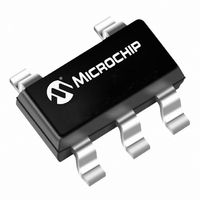
TC2014-2.7VCTTR Microchip Technology, TC2014-2.7VCTTR Datasheet - Page 3

TC2014-2.7VCTTR
Manufacturer Part Number
TC2014-2.7VCTTR
Description
IC CMOS LDO 2.7V 50MA SOT23A-5
Manufacturer
Microchip Technology
Specifications of TC2014-2.7VCTTR
Regulator Topology
Positive Fixed
Voltage - Output
2.7V
Voltage - Input
Up to 6V
Voltage - Dropout (typical)
0.045V @ 50mA
Number Of Regulators
1
Current - Output
50mA (Min)
Operating Temperature
-40°C ~ 125°C
Mounting Type
Surface Mount
Package / Case
SOT-23-5, SC-74A, SOT-25
Number Of Outputs
1
Polarity
Positive
Input Voltage Max
6 V
Output Voltage
2.7 V
Output Type
Fixed
Dropout Voltage (max)
140 / 210 mV
Output Current
50 mA
Line Regulation
0.05 %
Load Regulation
0.33 %
Voltage Regulation Accuracy
0.4 %
Maximum Power Dissipation
0.318 W
Maximum Operating Temperature
+ 125 C
Mounting Style
SMD/SMT
Minimum Operating Temperature
- 40 C
Lead Free Status / RoHS Status
Lead free / RoHS Compliant
Current - Limit (min)
-
Lead Free Status / Rohs Status
Lead free / RoHS Compliant
Other names
TC20142.7VCTTR
Available stocks
Company
Part Number
Manufacturer
Quantity
Price
Part Number:
TC2014-2.7VCTTR
Manufacturer:
MICROCHIP/微芯
Quantity:
20 000
ELECTRICAL CHARACTERISTICS (CONTINUED)
2004 Microchip Technology Inc.
Electrical Specifications: Unless otherwise specified, V
BOLDFACE type specifications apply for junction temperature of -40°C to +125°C.
Shutdown Supply
Current
Power Supply
Rejection Ratio
Output Short Circuit
Current
Thermal Regulation
Output Noise
Response Time,
(Note 8)
(from Shutdown Mode)
SHDN Input
SHDN Input High
Threshold
SHDN Input Low
Threshold
Note 1: The minimum V
Parameters
2: V
3:
4: Regulation is measured at a constant junction temperature using low duty cycle pulse testing. Load regulation is tested
5: Dropout Voltage is defined as the input-to-output differential at which the output voltage drops 2% below its nominal
6: Thermal Regulation is defined as the change in output voltage at a time T after a change in power dissipation is applied,
7: The maximum allowable power dissipation is a function of ambient temperature, the maximum allowable junction
8: Time required for V
over a load range from 1.0 mA to the maximum specified output current. Changes in output voltage due to heating
effects are covered by the Thermal Regulation specification.
value.
excluding load or line regulation effects. Specifications are for a current pulse equal to I
temperature and the thermal resistance from junction-to-air (i.e. T
R
TCV
is the regulator output voltage setting. For example: V
OUT
=
--------------------------------------------------------------------------- -
V
IN
V
OUTMAX
I
PSRR
OUTSC
OUT
has to meet two conditions: V
Sym
I
INSD
V
OUT
eN
V
T
IH
R
IL
/ P
to reach 95% of V
V
–
D
OUT
V
OUTMIN
T
Min
60
—
—
—
—
—
—
—
10
6 –
R
(output voltage setting), after V
IN
0.05
0.04
Typ
160
200
55
60
—
—
IN
= V
= 2.7V and V
R
+ 1V, I
R
Max
300
0.5
= 1.8V, 2.7V, 2.8V, 2.85V, 3.0V, 3.3V.
15
—
—
—
—
—
L
= 100 µA, C
IN
A
= V
, T
TC2014/2015/2185
nV/ Hz I
J
Units
%V
%V
R
µsec
V/W
,
mA
µA
dB
+ V
JA
IN
IN
OUT
SHDN
).
DROPOUT
SHDN = 0V
F
V
Note 6, Note 7
470 pF from Bypass to GND
V
C
V
V
= 3.3 µF, SHDN > V
L
OUT
IN
IN
IN
IN
= I
is switched from 0 to V
1 kHz, Cbypass = 0.01 µF
= 4V, I
= 2.5V to 6.0V
= 2.5V to 6.0V
= 1 µF, C
OUTMAX
.
= 0V
MAX
L
= 30 mA,
, F = 10 kHz
OUT
at V
Conditions
IN
= 10 µF
IH
= 6V for T = 10 msec.
, T
DS21662D-page 3
A
IN
= +25°C.
.


