LP38511TS-1.8/NOPB National Semiconductor, LP38511TS-1.8/NOPB Datasheet - Page 4
LP38511TS-1.8/NOPB
Manufacturer Part Number
LP38511TS-1.8/NOPB
Description
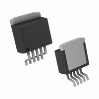
IC REG LDO 800MA EFLAG TO263-5
Manufacturer
National Semiconductor
Datasheet
1.LP38511TS-1.8EV.pdf
(14 pages)
Specifications of LP38511TS-1.8/NOPB
Regulator Topology
Positive Fixed
Voltage - Output
1.8V
Voltage - Input
2.25 ~ 5.5 V
Voltage - Dropout (typical)
0.135V @ 800mA
Number Of Regulators
1
Current - Output
800mA (Max)
Operating Temperature
-40°C ~ 125°C
Mounting Type
Surface Mount
Package / Case
TO-263-5, D²Pak (5 leads + Tab), TO-263BA
For Use With
LP38511TS-1.8EV - BOARD EVAL FOR LP38511TS-1.8LP38511S-1.8EV - BOARD EVAL FOR LP38511S-1.8 VREG
Lead Free Status / RoHS Status
Lead free / RoHS Compliant
Current - Limit (min)
-
Other names
LP38511TS-1.8


www.national.com
ERROR Flag
AC Parameters
Thermal Characteristics
V
Note 1: Absolute Maximum Ratings indicate limits beyond which damage to the device may occur. Operating Ratings indicate conditions for which the device is
intended to be functional, but does not guarantee specific performance limits. For guaranteed specifications and conditions, see the Electrical Characteristics.
Note 2: The human body model is a 100pF capacitor discharged through a 1.5kΩ resistor into each pin. Test method is per JESD22-A114.
Note 3: Refer to JEDEC J-STD-020C for surface mount device (SMD) package reflow profiles and conditions. Unless otherwise stated, the temperatures and
times are for Sn-Pb (STD) only.
Note 4: Device operation must be evaluated, and derated as needed, based on ambient temperature (T
junction temperature (T
Note 5: Output voltage line regulation is defined as the change in output voltage from the nominal value (ΔV
(ΔV
Note 6: Output voltage load regulation is defined as the change in output voltage from the nominal value (ΔV
(ΔI
Note 7: The line and load regulation specification contains only the typical number. However, the limits for line and load regulation are included in the output
voltage tolerance specification.
Note 8: Dropout voltage is defined as the minimum input to output differential voltage at which the output drops 2% below the nominal value. For the LP38511-1.8,
the minimum V
Note 9: The ERROR Flag thresholds are specified as percentage of the nominal regulated output voltage. See Application Information.
ERROR(SAT)
Symbol
PSRR
OUT
ΔT
IN
V
T
θ
θ
e
I
t
).
SD
TH
lk
JA
JC
d
).
n
SD
IN
Error Flag Threshold
(Note 9)
ERROR Flag Saturation
Voltage
ERROR Flag Pin Leakage
Current
ERROR Flag Delay time
Ripple Rejection
Output Noise Density
Output Noise Voltage
Thermal Shutdown
Thermal Shutdown Hysteresis T
Thermal Resistance
Junction to Ambient
(Note 4)
Thermal Resistance
Junction to Case
operating voltage is the limiting factor.
J(MAX)
), and package thermal resistance (θ
Parameter
V
ERROR Flag goes high
V
ERROR Flag goes low
I
V
V
f = 120Hz
V
f = 1 kHz
f = 120Hz
BW = 100Hz – 100kHz
T
TO-263 and TO-263 THIN
PSOP-8
TO-263 and TO-263 THIN
PSOP-8
SINK
OUT
OUT
ERROR
IN
IN
J
J
rising
falling from T
= 2.5V
= 2.5V
= 1 mA
rising threshold where
falling threshold where
JA
= 5.5V
).
Conditions
SD
4
A
), power dissipation (P
Min
78
74
OUT
-
-
-
-
-
-
-
-
-
-
-
-
-
OUT
) due to a change in the load current at the output
) due to a change in the voltage at the input
12.5
Typ
165
168
90
85
73
73
75
10
60
11
1
1
2
3
D
), maximum allowable operating
Max
98
93
45
-
-
-
-
-
-
-
-
-
-
-
-
µV (rms)
nV/
Units
°C/W
°C/W
mV
nA
dB
°C
µs
%
√
Hz
Related parts for LP38511TS-1.8/NOPB
Image
Part Number
Description
Manufacturer
Datasheet
Request
R

Part Number:
Description:
BOARD EVAL FOR LP38511TS-1.8
Manufacturer:
National Semiconductor
Datasheet:
Part Number:
Description:
National Semiconductor [8-Bit D/A Converter]
Manufacturer:
National Semiconductor
Datasheet:
Part Number:
Description:
National Semiconductor [Media Coprocessor]
Manufacturer:
National Semiconductor
Datasheet:
Part Number:
Description:
Digitally Controlled Tone and Volume Circuit with Stereo Audio Power Amplifier, Microphone Preamp Stage and National 3D Sound
Manufacturer:
National Semiconductor
Datasheet:
Part Number:
Description:
Digitally Controlled Tone and Volume Circuit with Stereo Audio Power Amplifier, Microphone Preamp Stage and National 3D Sound
Manufacturer:
National Semiconductor
Datasheet:
Part Number:
Description:
AC97 Rev 2 Codec with Sample Rate Conversion and National 3D Sound
Manufacturer:
National Semiconductor
Part Number:
Description:
Manufacturer:
National Semiconductor
Datasheet:
Part Number:
Description:
Manufacturer:
National Semiconductor
Datasheet:
Part Number:
Description:
General Purpose, Low Voltage, Low Power, Rail-to-Rail Output Operational Amplifiers
Manufacturer:
National Semiconductor
Datasheet:
Part Number:
Description:
8-bit 20 MSPS flash A/D converter.
Manufacturer:
National Semiconductor
Datasheet:
Part Number:
Description:
Low Noise Quad Operational Amplifier
Manufacturer:
National Semiconductor
Datasheet:
Part Number:
Description:
Quad Differential Line Receivers
Manufacturer:
National Semiconductor
Datasheet:
Part Number:
Description:
Quad High Speed Trapezoidal? Bus Transceiver
Manufacturer:
National Semiconductor
Datasheet:
Part Number:
Description:
Dual Line Receiver
Manufacturer:
National Semiconductor
Datasheet: